AMAZON multi-meters discounts AMAZON oscilloscope discounts
Until the last few decades of the twentieth century, ac machines tended to be employed primarily as single-speed devices. Typically they were operated from fixed-frequency sources (in most cases this was the 50or 60-Hz power grid). In the case of motors, control of motor speed requires a variable-frequency source, and such sources were not readily available. Thus, applications requiting variable speed were serviced by dc machines, which can provide highly flexible speed control, although at some cost since they are more complex, more expensive, and require more maintenance than their ac counterparts.
The availability of solid-state power switches changed this picture immensely.
It is now possible to build power electronics capable of supplying the variable-voltage/current, variable-frequency drive required to achieve variable-speed performance from ac machines. Ac machines have now replaced dc machines in many traditional applications, and a wide range of new applications have been developed.
As is the case with electro-mechanics and electric machinery, power electronics is a discipline which can be mastered only through significant study. Many books have been written on this subject, a few of which are listed in the bibliography at the end of this section. It is clear that a single section in a guide on electric machinery cannot begin to do justice to this topic. Thus our objectives here are limited. Our goal is to provide an overview of power electronics and to show how the basic building blocks can be assembled into drive systems for ac and dc machines. We will not focus much attention on the detailed characteristics of particular devices or on the many details required to design practical drive systems. In Section 11, we will build on the discussion of this section to examine the characteristics of some common drive systems.
1. POWER SWITCHES
Common to all power-electronic systems are switching devices. Ideally, these devices control current much like valves control the flow of fluids: turn them "ON," and they present no resistances to the flow of current; turn them "OFF," and no current flow is possible. Of course, practical switches are not ideal, and their specific characteristics significantly affect their applicability in any given situation. Fortunately, the essential performance of most power-electronic circuits can be understood assuming the switches to be ideal. This is the approach which we will adopt in this guide. In this section we will briefly discuss some of the common switching devices and present simplified, idealized models for them.
1.1 Diodes
Diodes constitute the simplest of power switches. The general form of the v-i characteristics of a diode is shown in FIG. 1.
The essential features of a diode are captured in the idealized v-i characteristic of FIG. 2a. The symbol used to represent a diode is shown in FIG. 2b along with the reference directions for the current i and voltage v. Based upon terminology developed when rectifier diodes were electron tubes, diode current flows into the anode and flows out of the cathode.
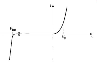
FIG. 1 v-i characteristic of a diode.
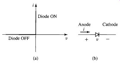
FIG. 2 (a) v-i characteristic of an ideal diode. (b) Diode symbol.
We can see that the ideal diode blocks current flow when the voltage is negative (i = 0 for v < 0) and passes positive current without voltage drop (v 0 for i > 0). We will refer to the negative-voltage region as the diode's OFF state and the positive-current region as the diode's ON state. Comparison with the v-i characteristic shows that a practical diode varies from an ideal diode in that:
There is a finite forward voltage drop, labeled VF in FIG. 1, for positive current flow. For low-power devices, this voltage range is typically on the order of 0.6-0.7 V while for high-power devices it can exceed 3 V. Corresponding to this voltage drop is a power dissipation. Practical diodes have a maximum power dissipation (and a corresponding maximum current) which must not be exceeded.
A practical diode is limited in the negative voltage it can withstand. Known as the reverse-breakdown voltage and labeled VRB in FIG. 1, this is the maximum reverse voltage that can be applied to the diode before it starts to conduct reverse current.
The diode is the simplest power switch in that it cannot be controlled; it simply turns ON when positive current begins to flow and turns OFF when the current attempts to reverse. In spite of this simple behavior, it is used in a wide variety of applications, the most common of which is as a rectifier to convert ac to dc.
The basic performance of a diode can be illustrated by the simple example shown in Example 1.
1.2 Silicon Controlled Rectifiers and TRIACs
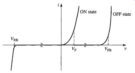
FIG. 4 v-i characteristic of an SCR.
FIG. 5 (a) Idealized SCR
v-i characteristic. (b) SCR symbol.
The characteristics of a silicon controlled rectifier, or SCR, also referred to as a thyristor, are similar to those of a diode. However, in addition to an anode and a cathode, the SCR has a third terminal known as the gate. FIG. 4 shows the form of the v-i characteristics of a typical SCR. As is the case with a diode, the SCR will turn ON only if the anode is positive with respect to the cathode. Unlike a diode, the SCR also requires a pulse of current iG into the gate to turn ON. Note however that once the SCR turns ON, the gate signal can be removed and the SCR will remain ON until the SCR current drops below a small value referred to as the holding current, at which point it will turn OFF just as a diode does.
As can be seen from FIG. 4, the ON-state characteristic of an SCR is similar to that of a diode, with a forward voltage drop VF and a reverse-breakdown voltage VRB. When the SCR is OFF, it does not conduct current over its normal operating range of positive voltage. However it will conduct if this voltage exceeds a characteristic voltage, labeled VFB in the figure and known as the forward-breakdown voltage. As is the case for a diode, a practical SCR is limited in its current-carrying capability.
For our purposes, we will simplify these characteristics and assume the SCR to have the idealized characteristics of FIG. 5a. Our idealized SCR appears as an open-circuit when it is OFF and a short-circuit when it is ON. It also has a holding current of zero; i.e., it will remain ON until the current drops to zero and attempts to go negative. The symbol used to represent an SCR is shown in FIG. 5b.
Care must be taken in the design of gate-drive circuitry to insure that an SCR turns on properly; e.g., the gate pulse must inject enough charge to fully turn on the SCR, and so forth. Similarly, an additional circuit, typically referred to as a snubber circuit, may be required to protect an SCR from being turned on inadvertently, such as might occur if the rate of rise of the anode-to-cathode voltage is excessive. Although these details must be properly accounted for to achieve successful SCR performance in practical circuits, they are not essential for the present discussion.
The basic performance of an SCR can be understood from the following example.
1.3 Transistors
For power-electronic circuits where control of voltages and currents is required, power transistors have become a common choice for the controllable switch. Although a number of types are available, we will consider only two: the metal-oxide-semiconductor field effect transistor (MOSFET) and the insulated-gate bipolar transistor (IGBT).
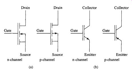
FIG. 11 (a) Symbols for nand p-channel MOSFETs. (b) Symbols for nand p-channel
IGBTs.
MOSFETs and IGBTs are both three-terminal devices. FIG. 11 a shows the symbols for nand p-channel MOSFETs, while FIG. 11 b shows the symbol for nand p-channel IGBTs. In the case of the MOSFET, the three terminals are referred to as the source, drain, and gate, while in the case of the IGBT the corresponding terminals are the emitter, collector, and gate. For the MOSFET, the control signal is the gate-source voltage, vGS. For the IGBT, it is the gate-emitter voltage, VGE. In both the MOSFET and the IGBT, the gate electrode is capacitively coupled to the remainder of the device and appears as an open circuit at dc, drawing no current, and drawing only a small capacitive current under ac operation.
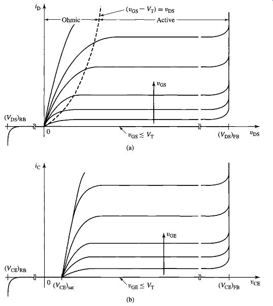
FIG. 12 (a) Typical v-i characteristic for an n-channel MOSFET. (b)
Typical v-i characteristic for an n-channel IGBT.
FIG. 12a shows the v-i characteristic of a typical n-channel MOSFET. The characteristic of the corresponding p-channel device looks the same, with the exception that the signs of the voltages and the currents are reversed. Thus, in an n-channel device, current flows from the drain to the source when the drain-source and gate-source voltages are positive, while in a p-channel device current flows from the source to the drain when the drain-source and gate-source voltages are negative.
Note the following features of the MOSFET and IGBT characteristics: m In the case of the MOSFET, for positive drain-source voltage vDS, no drain current will flow for values of VGS less than a threshold voltage which we will refer to by the symbol VT. Once vGS exceeds VT, the drain current iD increases as VGS is increased.
In the case of the IGBT, for positive collector-emitter voltage vCE, no collector current will flow for values of VGE less than a threshold voltage VT. Once VGE exceeds VT, the collector current ic increases as VGE is increased.
In the case of the MOSFET, no drain current flows for negative drain-source voltage.
In the case of the IGBT, no collector current flows for negative collector-emitter voltage.
Finally, the MOSFET will fail if the drain-source voltage exceeds its breakdown limits; in FIG. 12a, the forward breakdown voltage is indicated by the symbol (VDS)FB while the reverse breakdown voltage is indicated by the symbol ( VDS)RB. Similarly, the IGBT will fail if the collector-emitter voltage exceeds its breakdown values; in FIG. 12b, the forward breakdown voltage is indicated by the symbol (VcE)FB while the reverse breakdown voltage is indicated by the symbol (VcE)R B . m Although not shown in the figure, a MOSFET will fail due to excessive gate-source voltage as well as excessive drain current which leads to excessive power dissipation in the device. Similarly an IGBT will fail due to excessive gate-emitter voltage and excessive collector current.
Note that for small values of 1)CE , the IGBT voltage approaches a constant value, independent of the drain current. This saturation voltage, labeled ( VCE)sat in the figure, is on the order of a volt or less in small devices and a few volts in high-power devices.
Correspondingly, in the MOSFET, for small values of Vos, VDS is proportional to the drain current and the MOSFET behaves as a small resistance whose value decreases with increasing vGS. Fortunately, for our purposes, the details of these characteristics are not important. As we will see in the following example, with a sufficient large gate signal, the voltage drop across both the MOSFET and the IGBT can be made quite small. In this case, these devices can be modeled as a short circuit between the drain and the source in the case of the MOSFET and between the collector and the emitter in the case of the IGBT. Note, however, these "switches" when closed carry only unidirectional current, and hence we will model them as a switch in series with an ideal diode. This ideal-switch model is shown in FIG. 13a.
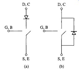
FIG. 13 (a) Ideal-switch model for a MOSFET or an IGBT showing the
series ideal diode which represents the unidirectional-current device
characteristic. (b) Ideal-switch model for devices which include a reverse-biased
protection diode. The symbols G, D, and S apply to the MOSFET while the
symbols B, C, and E apply to the IBGT.
In many cases, these devices are commonly protected by reverse-biased protection diodes connected between the drain and the source (in the case of a MOSFET) or between the collector and emitter (in the case of an IGBT). These protection devices are often included as integral components within the device package. If these protection diodes are included, there is actually no need to include the series diode, in which case the model can be reduced to that of FIG. 13b.
Example 4 shows that when a sufficiently large gate voltage is applied, the voltage drop across a power transistor can be reduced to a small value. Under these conditions, the IGBT will look like a constant voltage while the MOSFET will appear as a small resistance. In either case, the voltage drop will be small, and it is sufficient to approximate it as a closed switch (i.e., the transistor will be ON). When the gate drive is removed (i.e., reduced below VT), the switch will open and the transistor will turn OFE
2. RECTIFICATION: CONVERSION OF AC TO DC
The power input to many motor-drive systems comes from a constant-voltage, constant-frequency source (e.g., a 50or 60-Hz power system), while the output must provide variable-voltage and/or variable-frequency power to the motor. Typically such systems convert power in two stages: the input ac is first rectified to dc, and the dc is then converted to the desired ac output waveform. We will thus begin with a discussion of rectifier circuits. We will then discuss inverters, which convert dc to ac, in Sect. 3.
2.1 Single-Phase, Full-Wave Diode Bridge
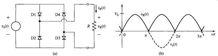
FIG. 15 (a) Full-wave bridge rectifier. (b) Resistor voltage.
Example 1 illustrates a half-wave rectifier circuit. Such rectification is typically used only in small, low-cost, low-power applications. Full-wave rectifiers are much more common. Consider the full-wave rectifier circuit of FIG. 15a. Here the resistor R is supplied from a voltage source Vs (t) = V0 sin cot through four diodes connected in a full-wave bridge configuration.
If we assume the diodes to be ideal, we can use the method-of-assumed states to show that the allowable diode states are:
Diodes D1 and D3 ON, diodes D2 and D4 OFF for Vs(t) > 0 Diodes D2 and D4 ON, diodes D1 and D3 OFF for Vs(t) < 0
The resistor voltage, plotted in FIG. 15b, is then given by:

(Eq. 1)
Now notice that the resistor voltage is positive for both polarities of the source voltage, hence the terminology full-wave rectification. The dc or average value of this waveform can be seen to be twice that of the half-wave rectified waveform of Example 1.
(Eq. 2)
The rectified waveforms of Figs. 3b and 15b are clearly not the sort of "dc" waveforms that are considered desirable for most applications. Rather, to be most useful, the rectified dc should be relatively constant and ripple free. Such a waveform can be achieved using a filter capacitor, as illustrated in Example 5.
In Example 5 we have seen that a capacitor can significantly decrease the ripple voltage across a resistive load. However, this comes at the cost of large bridge current pulses since the current must be delivered to the capacitor in the short time period during which the rectified source voltage is near its peak value.
FIG. 18 shows the addition of an inductor L at the output of the bridge, in series with the filter capacitor and its load. If the impedance of the inductor is chosen to be large compared to that of the capacitor/load combination at the frequency of the rectified source voltage, very little of the ac component of the rectified source voltage will appear across the capacitor, and thus the resultant L-C filter will produce low voltage ripple while drawing a relatively constant current from the diode bridge.
We have seen how the addition of a filter capacitor across a dc load can significantly reduce the ripple voltage seen by the load. In fact, the addition of significant capacitance can "stiffen" the rectified voltage to the point that it appears as a constant-voltage dc source to a load. In an analogous fashion, an inductor in series with a load will reduce the current ripple out of a rectifier. Under these conditions, the rectified source will appear as a constant-current dc source to a load.
The combination of a rectifier and an inductor at the output to supply a constant dc current to a load is of significant importance in power-electronic applications. It can be used, for example, as the front end of a current-source inverter which can be used to supply ac current waveforms to a load. We will investigate the behavior of such rectifier systems in the next section.
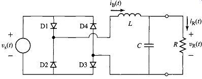
FIG. 18 Full-wave bridge rectifier with an L-C filter supplying a
resistive load.
2.2 Single-Phase Rectifier with Inductive Load
In this section we will examine the performance of a single-phase rectifier driving an inductive load. This situation covers both the case where the inductor is included as part of the rectifier system as a filter to smooth out current pulses as well as the case where the load itself is primarily inductive.
Let us examine first the half-wave rectifier circuit of FIG. 19. Here, the load consists of an inductor L in series with a resistor R. The source voltage is equal to:
Vs(t) = V0 cos o)t.
Consider first the case where L is small (wL << R). In this case, the load looks essentially resistive and the load current iL (t) will vary only slightly from the current for a purely resistive load as seen in Example 1. This current, obtained from a detailed analytical solution, is plotted in FIG. 20a, along with the current for a purely resistive load.
Note that the effect of the inductance is to decrease both the initial rate of rise of the current and the peak current. More significantly, the diode conduction angle increases; current flows for longer than the half-period that is the case for a purely resistive load. As can be seen in FIG. 20a, this effect increases as the inductance is increased; current flows for a greater fraction of the cycle, and the peak current as well as the current ripple is reduced.
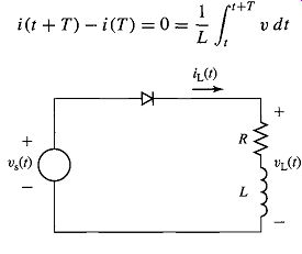
FIG. 19 Half-wave rectifier with an inductive load.
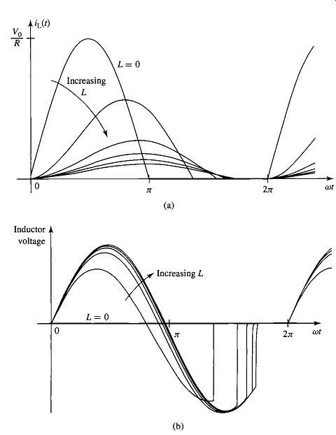
FIG. 20 Effect of increasing the series inductance in the circuit
of FIG. 19 on (a) the load current and (b) the inductor voltage.
FIG. 20b, which shows the inductor voltage, illustrates an important point that applies to all situations in which an inductor is subjected to steady-state, periodic conditions: the time-averaged voltage across the inductor must equal zero. This can be readily seen from the basic v-i relationship for an inductor:

(Eq. 3)
If we consider the operation of an inductor over a period of the excitation frequency and recognize that, under steady-state conditions, the change in the inductor current over that period must equal zero (i.e., it must have the same value at time t at the beginning of the period as it does one period later at time t + T), then we can write ...
... from which we can see that the net volt-seconds (and correspondingly the average voltage) across the inductor during a cycle must equal zero...

(Eq. 4)

(Eq. 5)
For this half-wave rectifier, note that as the inductance increases both the ripple current and the dc current will decrease. In fact, for large inductance (wL >> R) the dc load current will tend towards zero. This can be easily seen by the following argument: As the inductance increases, the conduction angle of the diode will increase from 180 ° and approach 360 ° for large values of L. In the limit of a 360 ° conduction angle, the diode can be replaced by a continuous short circuit, in which case the circuit reduces to the ac voltage source connected directly across the series combination of the resistor and the inductor.
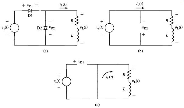
FIG. 21 (a) Half-wave rectifier with an inductive load and a free-wheeling
diode. (b) Equivalent circuit when Vs(t) > 0 and diode D1 is conducting.
(c) Equivalent circuit when Vs(t) < 0 and the free-wheeling diode D2
is conducting.
Under this situation, no dc current will flow since the source is purely ac. In addition, since the impedance Z = R + jwL becomes large with large L, the ac (tipple) current will also tend to zero.
FIG. 21a shows a simple modification which can be made to the half-wave rectifier circuit of FIG. 19. The free-wheeling diode D2 serves as an alternate path for inductor current.
To understand the behavior of this circuit, consider the condition when the source voltage is positive, and the rectifier diode D1 is ON. The equivalent circuit for this operating condition is shown in FIG. 2 lb. Note that under this condition, the voltage across diode D2 is equal to the negative of the source voltage and diode D2 is turned OFE.
This operating condition will remain in effect as long as the source voltage is positive. However, as soon as the source voltage begins to go negative, the voltage across diode D2 will begin to go positive and it will turn ON. Since the load is inductive, a positive load current will be flowing at this time, and that load current will immediately transfer to the short circuit corresponding to diode D2. At the same time, the current through diode D 1 will immediately drop to zero, diode D 1 will be reverse biased by the source voltage, and it will turn OFF. This operating condition is shown in FIG. 21 c. Thus, the diodes in this circuit alternately switch ON and OFF each half cycle: D1 is ON when Vs(t) is positive, and D2 is ON when it is negative.
Based upon this discussion, we see that the voltage VL (t) across the load (equal to the negative of the voltage across diode D2) is a half-wave rectified version of Vs(t) as seen in FIG. 22a. As shown in Example 1, the average of this voltage is Vdc = Vo/rr. Furthermore, the average of the steady-state voltage across the inductor must equal zero, and hence the average of the voltage VL (t) will appear across the resistor. Thus the dc load current will equal Vo/(rc R). This value is independent of the inductor value and hence does not approach zero as the inductance is increased.
FIG. 22b shows the diode and load currents for a relatively small value of inductance (coL < R), and FIG. 22c shows these same currents for a large inductance coL >> R. In each case we see the load current, which must be continuous due to the presence of the inductor, instantaneously switching between the diodes depending on the polarity of the source voltage. We also see that during the time diode D1 is ON, the load current increases due to the application of the sinusoidal source voltage, while during the time diode D2 is ON, the load current simply decays with the L/R time constant of the load itself.
As expected, in each case the average current through the load is equal to Vo/(Jr R). In fact, the presence of a large inductor can be seen to reduce the tipple current to the point that the load current is essentially a dc current equal to this value.
Let us now consider the case where the half-wave bridge of FIG. 19 is replaced by a full-wave bridge as in FIG. 23a. In this circuit, the voltage applied to the load is the full-wave-rectified source voltage as shown in FIG. 15 and the average (dc) voltage applied to the load will equal 2 Vo/zr. Here again, the presence of the inductor will tend to reduce the ac ripple. FIG. 24, again obtained from a detailed analytical solution, shows the current through the resistor as the inductance is increased.
If we assume a large inductor (wL >> R), the load current will be relatively ripple free and constant. It is therefore common practice to analyze the performance of this circuit by replacing the inductor by a dc current source lac as shown in FIG. 23b, where lac = 2 V0/(zr R). This is a commonly used technique in the analysis of power-electronic circuits which greatly simplifies their analysis.
Under this assumption, we can easily show that the diode and source currents of this circuit are given by waveforms of FIG. 25. FIG. 25a shows the current through one pair of diodes (e.g., diodes D1 and D3), and FIG. 25b shows the source current i~ (t). The essentially constant load current lac flows through each pair of diodes for one half cycle and appears as a square wave of amplitude l, jc at the source.
In a fashion similar to that which we saw in the half-wave rectifier circuit with the free-wheeling diode, here a pair of diodes (e.g., diodes D 1 and D3) are carrying current when the source voltage reverses, turning ON the other pair of diodes and switching OFF the pair that were previously conducting. In this fashion, the load current remains continuous and simply switches between the diode pairs.
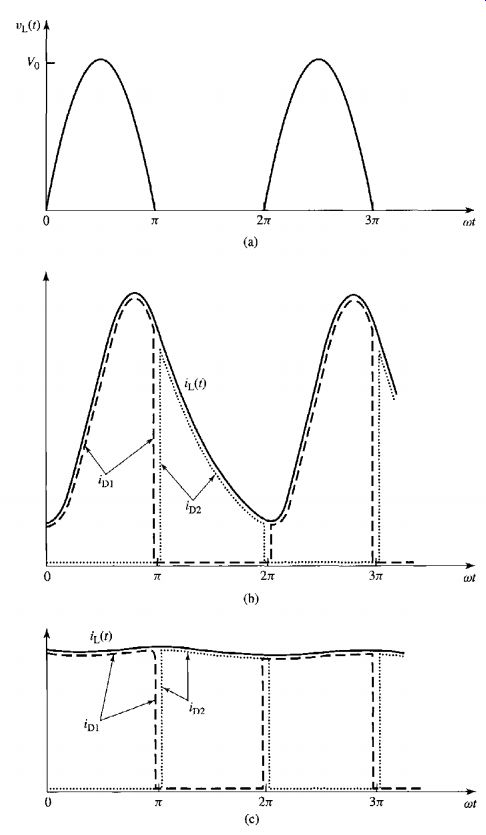
FIG. 22
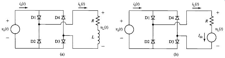
Fig. 23 (a) Full-wave rectifier with an inductive load. (b) Full-wave
rectifier with the inductor replaced by a dc current source.
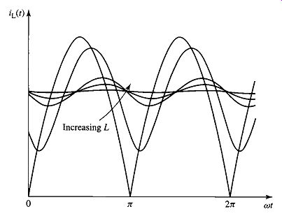
FIG. 24 Effect of increasing the series inductance in the circuit
of FIG. 23a on the load current.
2.3 Effects of Commutating Inductance
Our analysis and the current waveforms of FIG. 25 show that the current commutes instantaneously from one diode pair to the next. In practical circuits, due to the presence of source inductance, commutation of the current between the diode pairs does not occur instantaneously. The effect of source inductance, typically referred to as commutating inductance, will be examined by studying the circuit of FIG. 26 in which a source inductance Ls has been added in series with the voltage source in the full-wave rectifier circuit of FIG. 23b. We have again assumed that the load time constant is large (coL/R >> 1) and have replaced the inductor with a dc current source Idc.
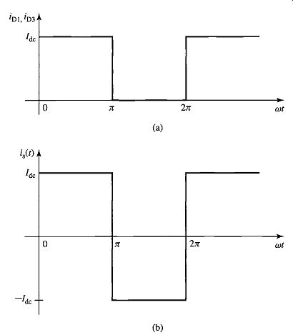
FIG. 25 (a) Current through diodes D1 and D3 and (b) source current
for the circuit of FIG. 23, both in the limit of large inductance.
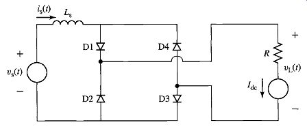
FIG. 26 Full-wave bridge rectifier with source inductance.
DC load current assumed.
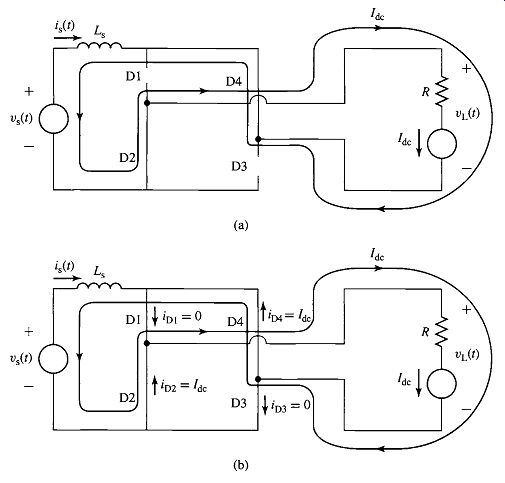
FIG. 27 (a) Condition of the full-wave circuit of FIG. 26 immediately
before diodes D1 and D3 turn ON. (b) Condition immediately after diodes
D1 and D3 turn ON.
FIG. 27a shows the situation which occurs when diodes D2 and D4 are ON and carrying current 10c and when Vs < 0. Commutation begins when Vs reaches zero and begins to go positive, turning ON diodes D 1 and D3. Note that because the current in the source inductance Ls cannot change instantaneously, the circuit condition at this time is described by FIG. 27b: the current through Ls is equal to --Idc, the current through diodes D2 and D4 is equal to/de, while the current through diodes D1 and D3 is zero.
Under this condition with all four diodes ON, the source voltage Vs(t) appears directly across the source inductance Ls. Noting that commutation starts at the time when Vs(t) 0, the current through Ls can be written as:
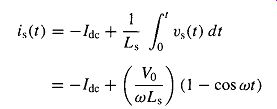
(Eq. 6)
Noting that is -iDI -iD4, that iD1 + iD2 = Idc and, that by symmetry, iD4 =iD2, we can write that

(Eq. 7)
Diode D2 (and similarly diode D4) will turn OFF when iD2 reaches zero, which will occur when is(t) Idc. In other words, commutation will be completed at time tc, when the current through Ls has completely reversed polarity and when all of the load current is flowing through diodes D 1 and D3.
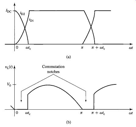
FIG. 28 (a) Currents through diodes D1 and D2 showing the finite commutation
interval. (b) Load voltage showing the commutation notches due to the finite
commutation time.
Setting is(tc) = Idc and solving Eq. 6 gives an expression for the commutation interval tc as a function of Idc
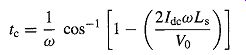
(Eq. 8)
FIG. 28a shows the currents through diodes D1 and D2 as the current commutates between them. The finite commutation time tc can clearly be seen. There is a second effect of commutation which can be clearly seen in FIG. 28b which shows the rectified load voltage VL (t). Note that during the time of commutation, with all the diodes on, the rectified load voltage is zero. These intervals of zero voltage on the rectified voltage waveform are known as commutation notches.
Comparing the ideal full-wave rectified voltage of FIG. 15b to the waveform of FIG. 28b, we see that the effect of the commutation notches is to reduce the dc output of the rectifier. Specifically, the dc voltage in this case is given by
(Eq. 9)
...where tc is the commutation interval as calculated by Eq. 8.
Finally, the dc load current can be calculated as function of tc […]
We have seen that commutating inductance (which is to a great extent unavoidable n practical circuits) gives rise to a finite commutation time and produces commutation notches in the rectified-voltage waveform which reduces the dc voltage applied to he load.
2.4 Single-Phase, Full-Wave, Phase-Controlled Bridge
FIG. 31 shows a full-wave bridge in which the diodes of FIG. 15 have been replaced by SCRs. We will assume that the load inductance L is sufficiently large that the load current is essentially constant at a dc value Idc. We will also ignore any effects of commutating inductance, although they clearly would play the same role in a phase-controlled rectifier system as they do in a diode-rectifier system.
FIG. 32 shows the source voltage and the timing of the SCR gate pulses under a typical operating condition for this circuit. Here we see that the firing pulses are delayed by an angle c~a after the zero-crossing of the source-voltage waveform, with the firing pulses for SCRs T 1 and T3 occurring after the positive-going transition of vs(t) and those for SCRs T2 and T4 occurring after the negative-going transition.
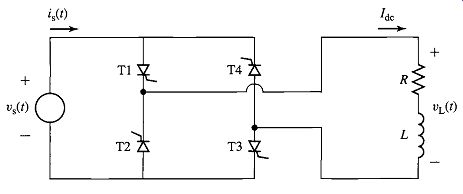
FIG. 31 Full-wave, phase-controlled SCR bridge.
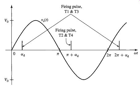
FIG. 32 Source voltage and firing pulses for th phase-controlled SCR
bridge of FIG. 31.
FIG. 33a shows the current through SCRs T1 and T3. Note that these SCRs do not turn ON until they receive firing pulses at angle Otd after they are forward biased following positive-going zero crossing of the source voltage. Furthermore, note that SCRs T2 and T4 do not turn ON following the next zero crossing of the source voltage.
Hence, SCRs T1 and T3 remain ON, carrying current until SCRs T2 and T4 are turned ON by gate pulses. Rather, T2 and T4 turn ON only after they receive their respective gate pulses (for example, at angle Jr + Otd in FIG. 33). This is an example of forced commutation, in that one pair of SCRs does not naturally commutate OFF but rather must be forcibly commutated when the other pair is turned ON.
[...]
2.5 Inductive Load with a Series DC Source
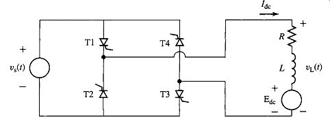
FIG. 35 Full-wave, phase-controlled SCR bridge with an inductive load
including a dc voltage source.
As we have seen in Section 9, dc motors can be modeled as dc voltage sources in series with an inductor and a resistor. Thus, it would be useful to briefly investigate the case of a dc voltage source in series with an inductive load.
Let us examine the full-wave, phase-controlled SCR rectifier system of FIG. 35.
Here we have added a dc source Edc in series with the load. Again assuming that coL >> R so that the load current is essentially dc, we see that the load voltage VL(t) depends solely on the timing of the SCR gate pulses and hence is unchanged by the presence of the dc voltage source Edc. Thus the dc value of VL(t) is given by Eq. 13 as before.
In the steady-state, the dc current through the load can be found from the net dc voltage across the resistor as...

(Eq. 18)
...where Vac is found from Eq. 13. Under transient conditions, it is the difference voltage, Vac Eac, that drives a change in the dc current through the series R-L combination, in a fashion similar to that illustrated in Example 7.
2.6 Three-Phase Bridges
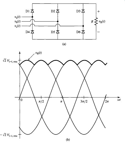
FIG. 36 (a) Three-phase, six-pulse diode bridge with resistive load. (b)
Line-to-line voltages and resistor voltage.
Although many systems with ratings ranging up to five or more kilowatts run off single-phase power, most large systems are supplied from three-phase sources. In general, all of the issues which we have discussed with regard to single-phase, full-wave bridges apply directly to situations with three-phase bridges. As a result, we will discuss three-phase bridges only briefly.
FIG. 36a shows a system in which a resistor R is supplied from a three-phase source through a three-phase, six-pulse diode bridge. FIG. 36b shows the three-phase line-to-line voltages (peak value ~/2Vl-i,rms where Vl-l, rms is the rms value of the line-to-line voltage) and the resistor voltage VR(t), found using the method-of-assumed-states and assuming that the diodes are ideal.
Note that VR has six pulses per cycle. Unlike the single-phase, full-wave bridge of FIG. 15a, the resistor voltage does not go to zero. Rather, the three-phase diode bridge produces an output voltage equal to the instantaneous maximum of the absolute value of the three line-to-line voltages. The dc average of this voltage (which can be obtained by integrating over 1/6 of a cycle) is given by
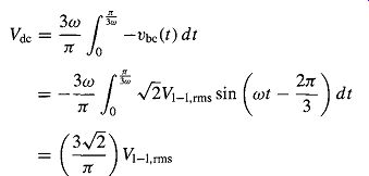
(Eq. 19)
...where Vl-l,rms is the rms value of the line-to-line voltage.
Table 1 shows the diode-switching sequence for the three-phase bridge of FIG. 36a corresponding to a single period of the three-phase voltage of waveforms of FIG. 36b. Note that only two diodes are on at any given time and that each diode is on for 1/3 of a cycle (120°). Analogous to the single-phase, full-wave, phase-controlled SCR bridge of Figs. 31 and 35, FIG. 37 shows a three-phase, phase-controlled SCR bridge.
Assuming continuous load current, corresponding for example to the condition coL >> R, in which case the load current will be essentially a constant dc current loc, this bridge is capable of applying a negative voltage to the load and of regenerating power in a fashion directly analogous to the single-phase, full-wave, phase-controlled SCR bridge which we discussed in Sect. 2.4.
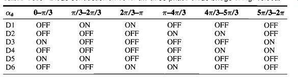
Table 1 Diode conduction times for the three-phase diode bridge of FIG.
36a.
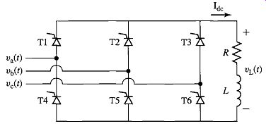
FIG. 37 Three-phase, phase-controlled SCR bridge circuit with an inductive
load.
It is a relatively straightforward matter to show that maximum output voltage of this bridge configuration will occur when the SCRs are turned ON at the times when the diodes in a diode bridge would naturally turn ON. These times can be found from Table 1. For example, we see that SCR T5 must be turned ON at angle C~d = 0 (i.e., at the positive zero crossing of Vab(t)). Similarly, SCR T1 must be turned ON at time C~d = Jr/3, and so on.
Thus, one possible scheme for generating the SCR gate pulses is to use the positive-going zero crossing of Vab(t) as a reference from which to synchronize a pulse train running at six times the fundamental frequency (i.e., there will be six uniformly-spaced pulses in each cycle of the applied voltage). SCR T5 would be fired first, followed by SCRs T1, T6, T2, T4, and T3 in that order, each separated by 60 ° in phase delay.
If the firing pulses are timed to begin immediately following the zero crossing of Vab(t) the load voltage waveform VL(t) will be that of FIG. 36b. If the firing pulses are delayed by an angle Otd, then the load-voltage waveforms will appear as in FIG. 38a (for Ctd = 0.1zr) and FIG. 38b (for Ctd = 0.9zr).
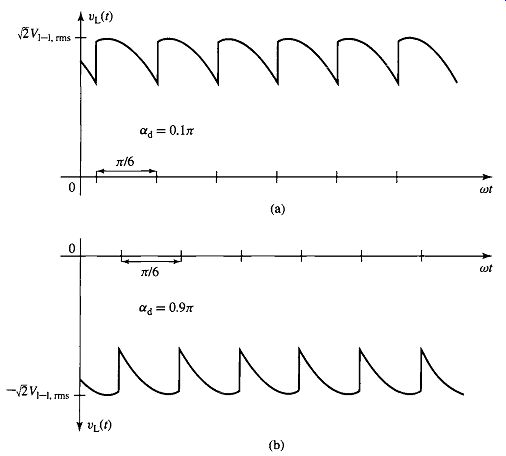
FIG. 38 Typical load voltages for delayed firing of the SCRs in the
three-phase, phase-controlled rectifier of FIG. 37 (a) Otd = 0.1rr, (b)
Re -" 0.97f.
The derivations for three-phase bridges presented here have ignored issues such as the effect of commutating inductance, which we considered during our examination of single-phase rectifiers. Although the limited scope of our presentation does not permit us to specifically discuss them here, the effects in three-phase rectifiers are similar to those for single-phase systems and must be considered in the design and analysis of practical three-phase rectifier systems.
3. INVERSION: CONVERSION OF DC TO AC
In Sect. 2 we discussed various rectifier configurations that can be used to convert ac to dc. In this section, we will discuss some circuit configurations, referred to as inverters, which can be used to convert dc to the variable-frequency, variable-voltage power required for many motor-drive applications. Many such configurations and techniques are available, and we will not attempt to discuss them all. Rather, consistent with the aims of this section, we will review some of the common inverter configurations and highlight their basic features and characteristics.
For the purposes of this discussion, we will assume the inverter is preceded by a "stiff" dc source. For example, in Sect. 2, we saw how an LC filter can be used to produce a relatively constant dc output voltage from a rectifier. Thus, as shown in FIG. 39a, for our study of inverters we will represent such rectifier systems by a constant dc voltage source V0, known as the dc bus voltage at the inverter input.
We will refer to such a system, with a constant-dc input voltage, as a voltage-source inverter.
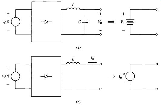
FIG. 39 Inverter-input representations. (a) Voltage source. (b) Current
source.
Similarly, we saw that a "large" inductor in series with the rectifier output produces a relatively constant dc current, known as the dc link current. We will therefore represent such a rectifier system by a current source I0 at the inverter input. We will refer to this type of inverter as a current-source inverter.
Note that, as we have seen in Sect. 2, the values of these dc sources can be varied by appropriate controls applied to the rectifier stage, such as the timing of gate pulses to SCRs in the rectifier bridge. Control of the magnitude of these sources in conjunction with controls applied to the inverter stage provides the flexibility required to produce a wide variety of output waveforms for various motor-drive applications.
3.1 Single-Phase, H-bridge Step-Waveform Inverters
FIG. 40a shows a single-phase inverter configuration in which a load (consisting here of a series RL combination) is fed from a dc voltage source V0 through a set of four IGBTs in what is referred to as an H-bridge configuration. MOSFETs or other switching devices are equally applicable to this configuration. As we discussed in Sect. 1.3, the IGBTs in this system are used simply as switches. Because the IGBTs in this H-bridge include protection diodes, we can analyze the performance of this circuit by replacing the IGBTs by the ideal-switch model of FIG. 13b as shown in FIG. 40b.
For our analysis of this inverter, we will assume that the switching times of this inverter (i.e., the length of time the switches remain in a constant state) are much longer than the load time constant L/R. Hence, on the time scale of interest, the load current will simply be equal to VL/R, with VL being determined by the state of the switches.
Let us begin our investigation of this inverter configuration assuming that switches S1 and $3 are ON and that iL is positive, as shown in FIG. 41a. Under this condition the load voltage is equal to V0 and the load current is thus equal to Vo/R. Let us next assume that switch S1 is turned OFF, while $3 remains ON. This will cause the load current, which cannot change instantaneously due to the presence of the inductor, to commutate from switch S 1 to diode D2, as shown in FIG. 4 lb.
Note that under this condition, the load voltage is zero and hence there will be zero load current. Note also that this same condition could have been reached by turning switch $3 OFF with S 1 remaining ON.
FIG. 40 Single-phase H-bridge inverter configuration. (a) Typical
configuration using IGBTs. (b) Generic configuration using ideal switches.
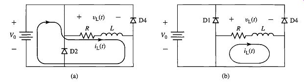
FIG. 41 Analysis of the H-bridge inverter of FIG. 40b. (a) Switches
S1 and S3 ON. (b) Switch S3 ON.
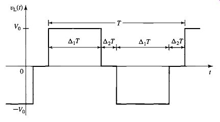
FIG. 42 Typical output-voltage waveform for the H-bridge of FIG. 40.
At this point, it is possible to reverse the load voltage and current by turning ON switches $2 and $4, in which case VL =V0 and iL =Vo/R. Finally, the current can be again brought to zero by turning OFF either switch $2 or switch $4. At this point, one cycle of an applied load-voltage waveform of the form of FIG. 42 has been completed.
A typical waveform produced by the switching sequence described above is shown in FIG. 42, with an ON time of Al T and OFF time of A2T (A 2 = 0.5 -A1) for both the positive and negative portions of the cycle. Such a waveform consists of a fundamental ac component of frequency f0 = 1/T, where T is the period of the switching sequence, and components at odd-harmonics frequencies of that fundamental.
The waveform of FIG. 42 can be considered a simple one-step approximation to a sinusoidal waveform. Fourier analysis can be used to show that it has a fundamental component of peak amplitude

(Eq. 21)
... and n'th-harmonic components (n = 3, 5, 7 .... ) of peak amplitude ...

(Eq. 22)
Although this stepped waveform appears to be a rather crude approximation to a sinusoid, it clearly contains a significant fundamental component. In many applications it is perfectly adequate as the output voltage of a motor-drive. For example, three-such waveforms, separated by 120 ° in time phase, could be used to drive a three-phase motor. The fundamental components would combine to produce a rotating flux wave as discussed in Section 4. In some motor-drive systems, LC filters, consisting of shunt capacitors operating in conjunction with the motor phase inductances, are used to reduce the harmonic voltages applied to the motor phase windings.
In general, the higher-order harmonics, whose amplitudes vary inversely with their harmonic number, as seen from Eq. 22, will produce additional core loss in the stator as well as dissipation in the rotor. Provided that these additional losses are acceptable both from the point of view of motor heating as well as motor efficiency, a drive based upon this switching scheme will be quite adequate for many applications.
3.2 Pulse-Width-Modulated Voltage-Source Inverters
Let us again consider the H-bridge configuration of FIG. 40b, repeated again in FIG. 45. Again, an RL load is fed from a voltage source through the H-bridge.
However, in this case, let us assume that the switching time of the inverter is much shorter than the load time constant (L/R). Consider a typical operating condition as shown in FIG. 46. Under this condition, the switches are operated with a period T and a duty cycle D (0 < D < 1). As can be seen from FIG. 46a, for a time DT switches S1 and $3 are ON, and the load voltage is V0. This is followed by a time (1 D)T during which switches S1 and $3 are OFF, and the current is transferred to diodes D2 and D4, setting the load voltage equal to -V0. The duty cycle D is thus a fraction of the total period, in this case the fraction of the period during which the load voltage is V0.
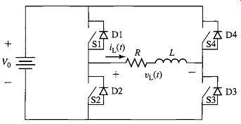
FIG. 45 Single-phase H-bridge inverter configuration.
Note that although switches $2 and $4 would normally be turned ON after switches S1 and $3 are turned OFF (but not before they are turned OFF, to avoid a direct short across the voltage source) because they are actually semiconductor devices, they will not carry any current unless the load current goes negative. Rather, the current will flow through the protection diodes D 1 and D3. Alternatively, if the load current is negative, then the current will be controlled by the operation of switches $2 and $4 in conjunction with diodes D 1 and D3. Under this condition, switches S 1 and $3 will not carry current.
This type of control is referred to as pulse-width modulation, or PWM, because it is implemented by varying the width of the voltage pulses applied to the load. As can be seen from FIG. 46a, the average voltage applied to the load is equal to:

(Eq. 23)
As we will now show, varying the duty cycle under PWM control can produce a continuously varying load current.
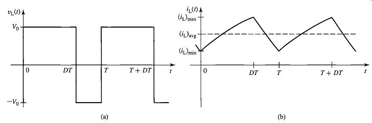
FIG. 46 Typical (a) voltage and (b) current waveform under PWM operation.
A typical load-current waveform is shown in FIG. 46b. In the steady state, the average current through the inductor will be constant and hence voltage across the inductor must equal zero. Thus, the average load current will equal the average
[...]
Now let us consider the situation for which the duty cycle is varied with time, i.e., D = D(t). If D(t) varies slowly in comparison to the period T of the switching frequency, from Eq. 23, the average load voltage will be equal to

(Eq. 33)
...and the average load current will be...
(Eq. 34)
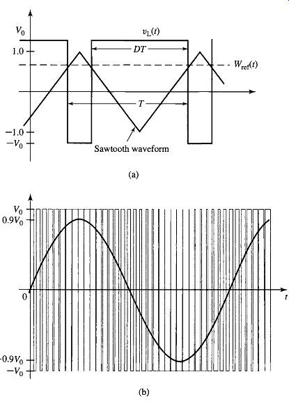
FIG. 47 (a) Method for producing a variable duty cycle from a reference
waveform Wref(t). (b) Load voltage and average load voltage for Wref(t)
= 0.9 sin cot.
FIG. 47a illustrates a method for producing the variable duty cycle for this system. Here we see a saw-tooth waveform which varies between -1 and 1. Also shown is a reference waveform Wref(t) which is constrained to lie within the range 1 and 1. The switches will be controlled in pairs. During the time that Wref(t) is greater than the saw-tooth waveform, switches S1 and $3 will be ON and the load voltage will be V0. Similarly, when Wref(t) is less than the saw-tooth waveform, switches $2
[...]
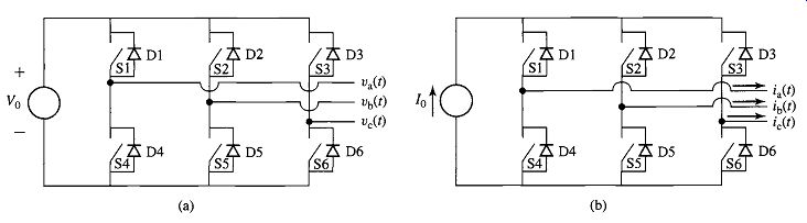
FIG. 48 Three-phase inverter configurations. (a) Voltage-source. (b)
Current-source.
Note that the H-bridge inverter configuration of FIG. 43 can be used to produce a PWM current-source inverter. In a fashion directly analogous to the derivation of Eq. 36, one can show that such an inverter would produce an average current of the form

(Eq. 37)
... where I0 is the magnitude of the dc link current feeding the H-bridge. Note, however, that the sudden current swings between I0 and -I0 associated with such an inverter will produce large voltages should the load have any inductive component. As a result, practical inverters of this type require large capacitive filters to absorb the harmonic components of the PWM current and to protect the load against damage due to voltage-induced insulation failure.
3.3 Three-Phase Inverters Although the single-phase motor drives of Sect. 3.2 demonstrate the important characteristics of inverters, most variable-frequency drives are three phase. Figures 48a and 48b show the basic configuration of three-phase motor inverters (voltage- and current-source respectively). Here we have shown the switches as ideal switches, recognizing that in a practical implementation, bidirectional capability will be achieved by a combination of a semiconductor switching device, such as an IGBT and a MOSFET, and a reverse-polarity diode.
These configurations can be used to produce both stepped waveforms (either voltage-source or current-source) as well as pulse-width-modulated waveforms. This will be illustrated in the following example.
4. SUMMARY
The goal of this section is relatively modest. Our focus has been to introduce some basic principles of power electronics and to illustrate how they can be applied to the design of various power-conditioning circuits that are commonly found in motor drives. Although the discussion in this section is neither complete nor extensive, it is intended to provide the background required to support the various discussions of motor control which are presented in this guide.
We began with a brief overview of a few of the available solid-state switching devices: diodes, SCRs, IGBTs and MOSFETs, and so on. We showed that, for the purposes of a preliminary analysis, it is quite sufficient to represent these devices as ideal switches. To emphasize the fact that they typically can pass only unidirectional current, we included ideal diodes in series with these switches. The simplest of these devices is the diode, which has only two terminals and is turned ON and OFF simply by the conditions of the external circuit. The remainder have a third terminal which can be used to turn the device ON and, in the case of transistors such as MOSFETS and IGBTs, OFF again.
A typical variable-frequency, variable-voltage motor-drive system can be considered to consist of three sections. The input section rectifies the power-frequency, fixed-voltage ac input and produces a dc voltage or current. The middle section filters the rectifier output, producing a relatively constant dc current or voltage, depending upon the type of drive under consideration. The output inverter section converts the dc to variable-frequency, variable-voltage ac voltages or currents which can be applied to the terminals of a motor.
The simplest inverters we investigated produce stepped voltage or current waveforms whose amplitude is equal to that of the dc source and whose frequency can be controlled by the timing of the inverter switches. To produce a variable-amplitude output waveform, it is necessary to apply additional control to the rectifier stage to vary the amplitude of the dc bus voltage or link current supplied to the inverter.
We also discussed pulse-width-modulated voltage-source inverters. In this type of inverter, the voltage to the load is switched between V0 and -V0 such that the average load voltage is determined by the duty cycle of the switching waveform.
Loads whose time constant is long compared to the switching time of the inverter will act as filters, and the load current will then be determined by the average load voltage. Pulse-width modulated current-source inverters were also discussed briefly.
The reader should approach the presentation here with great caution. It is important to recognize that a complete treatment of power electronics and motor drives is typically the topic of a multiple-course sequence of study. Although the basic principles discussed here apply to a wide range of motor drives, there are many details which must be included in the design of practical motor drives. Drive circuitry to turn ON the "switches" (gate drives for SCRs, MOSFETs, IGBTs, etc.) must be carefully designed to provide sufficient drive to fully turn on the devices and to provide the proper switching sequences. The typical inverter includes a controller and a protection system which is quite elaborate. Typically, the design of a specific drive is dominated by the current and voltage ratings of available switches devices. This is especially true in the case of high-power drive systems in which switches must be connected in series and/or parallel to achieve the desired power rating. The reader is referred to references in the bibliography for a much more complete discussion of power electronics and inverter systems than has been presented here.
Motor drives based upon the configurations discussed here can be used to control motor speed and motor torque. In the case of ac machines, the application of power-electronic based motor drives has resulted in performance that was previously available only with dc machines and has led to widespread use of these machines in most applications.
5. BIBLIOGRAPHY
This section is intended to serve as an introduction to the discipline of power electronics. For readers who wish to study this topic in more depth, this bibliography lists a few of the many textbooks which have been written on this subject.
Bird, B. M., K. G. King, and D. A. G. Pedder, An Introduction to Power Electronics, 2/e. New York: John Wiley & Sons, 1993.
Dewan, S. B., and A. Straughen, Power Semiconductor Circuits. New York: John Wiley & Sons, 1975.
Hart, D. W., Introduction to Power Electronics. Englewood Cliffs, New Jersey: Prentice-Hall, 1998.
Kassakian, J. G., M. E Schlecht, and G. C. Verghese, Principles of Power Electronics. Reading, Massachusetts: Addison-Wesley, 1991.
Mohan, N., T. M. Undeland, and W. P. Robbins, Power Electronics: Converters, Applications, and Design, 3/e. New York: John Wiley & Sons, 2002.
Rahsid, M. H., Power Electronics: Circuits, Devices and Applications, 2/e. Englewood Cliffs, New Jersey: Prentice-Hall, 1993.
Subrahmanyam, V., Electric Drives: Concepts and Applications. New York: McGraw-Hill, 1996.
Thorborg, K., Power Electronics. Englewood Cliffs, New Jersey: Prentice Hall International ( U.K.) Ltd, 1988.
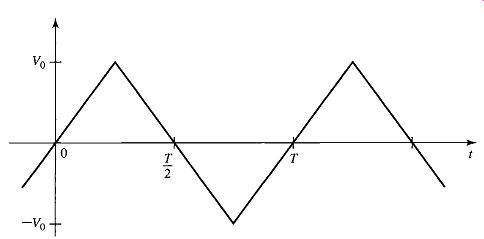
FIG. 50 Triangular voltage waveform.
6. QUIZ
1. Consider the half-wave rectifier circuit of FIG. 3a. The circuit is driven by a triangular voltage source Vs(t) of amplitude V0 = 9 V as shown in FIG. 50. Assuming the diode to be ideal and for a resistor R = 1.5 kohm:
a. Plot the resistor voltage VR(t).
b. Calculate the rms value of the resistor voltage.
c. Calculate the time-averaged power dissipation in the resistor.
2. Repeat Problem 1 assuming the diode to have a fixed 0.6 V voltage drop when it is ON but to be otherwise ideal. In addition, calculate the time-averaged power dissipation in the diode.
3. Consider the half-wave SCR rectifier circuit of FIG. 6 supplied from the triangular voltage source of FIG. 50. Assuming the SCR to be ideal, calculate the rms resistor voltage as a function of the firing-delay time td (0 < td < T/2). 10.4 Consider the rectifier system of Example 5. Write a MATLAB script to plot the ripple voltage as a function of filter capacitance as the filter capacitance is varied over the range 3000/xF < C < 105/xF. Assume the diode to be ideal. Use a log-scale for the capacitance.
5. Consider the full-wave rectifier system of FIG. 16 with R = 500 fl and C -200/xF. Assume each diode to have a constant voltage drop of 0.7 V when it is ON but to be otherwise ideal. For a 220 V rms, 50 Hz sinusoidal source, write a MATLAB script to calculate
a. the peak voltage across the load resistor.
b. the magnitude of the ripple voltage.
c. the time-averaged power supplied to the load resistor.
d. the time-averaged power dissipation in the diode bridge.
6. Consider the half-wave rectifier system of FIG. 51. The voltage source is Vs(t) -V0 sin oot where V0 = 15 V, and the frequency is 100 Hz. For L = 1 mH and R = 1 S2, plot the inductor current iL(t) for the first 1-1/2 cycles of the applied waveform assuming the switch closes at time t = 0. 10.7 Repeat Problem 6, using MATLAB to plot the inductor current for the first 10 cycles following the switch closing at time t -0. (Hint: This problem can be easily solved, using simple Euler integration to solve for the current.)
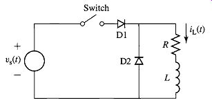
FIG. 51 Half-wave rectifier system for Problem 6.
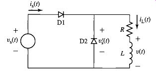
FIG. 52 Half-wave rectifier system for Problem 8.
8. Consider the half-wave rectifier system of FIG. 52 as L becomes sufficiently large such that co (L/R) >> 1, where co is the supply frequency. In this case, the inductor current will be essentially constant. For R 5 ohm and Vs(t) = V0 sin cot where V0 = 45 V and co = 100zr rad/sec. Assume the diodes to be ideal.
a. Calculate the average (dc) value Vdc of the voltage v' s (t) across the series resistor/inductor combination.
b. Using the fact that, in the steady state, there will be zero average voltage across the inductor, calculate the dc inductor current Idc.
c. Plot the instantaneous inductor voltage v(t) over one cycle of the supply voltage.
d. Plot the instantaneous source current is(t).
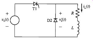
FIG. 53 Half-wave, phase-controlled rectifier system for Problem 9.
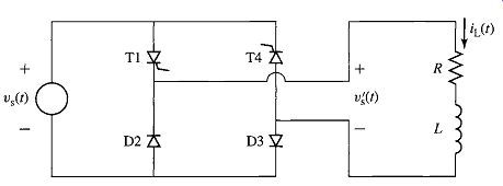
FIG. 54 Full-wave, phase-controlled rectifier system for Problem 10.
9. Consider the half-wave, phase-controlled rectifier system of FIG. 53. This is essentially the same circuit as that of Problem 8 with the exception that diode D1 of FIG. 52 has been replaced by an SCR, which you can consider to be ideal. Let R = 5 ~ and Vs(t) = V0 sin cot, where V0 = 45 V and co 100zr rad/sec. Assume that the inductor L is sufficiently large such that co(L/R) >> 1 and that the SCR is triggered ON at time td (0 < td < It/co).
a. Find an expression for the average (dc) value Vdc of the voltage v~ (t) across the series resistor/inductor combination as a function of the delay time to.
b. Using the fact that, in the steady state, there will be zero average voltage across the inductor, find an expression for the dc inductor current Idc, again as a function of the delay time td.
c. Plot Idc as a function of td for (0 < td < re/W).
10. The half-wave, phase-controlled rectifier system of Problem 9 and FIG. 53 is to be replaced by the full-wave, phase-controlled system of FIG. 54. SCR T1 will be triggered ON at time ta (0 < td < re/co), and SCR T4 will be triggered on exactly one half cycle later.
a. Find an expression for the average (dc) value Vdc of the voltage v~ (t) across the series resistor/inductor combination as a function of the delay time td.
b. Using the fact that, in the steady state, there will be zero average voltage across the inductor, find an expression for the dc inductor current Idc, again as a function of the delay time td.
c. Plot Idc as a function of td for (0 < td _< re/co).
d. Plot the source current is(t) for one cycle of the source voltage for td = 3 msec.
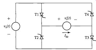
FIG. 55 Full-wave, phase-controlled rectifier for Problem 11.
11. The full-wave, phase-controlled rectifier of FIG. 55 is supplying a highly inductive load such that the load current can be assumed to be purely dc, as represented by the current source Idc in the figure. The source voltage is a sinusoid, Vs(t) = V0 sinwt. As shown in FIG. 31, SCRs T1 and T3 are triggered together at delay angle Otd (0 < c~d < Jr), and SCRs T2 and T4 are triggered exactly one-half cycle later.
a. For c~d = n/4: (i) Sketch the load voltage v~(t). (ii) Calculate the average (dc) value Vdc of V's(t). (iii) Calculate the time-averaged power supplied to the load.
b. Repeat part (a) for otd = 3:r/4.
12. A full-wave diode rectifier is fed from a 50-Hz, 220-V rms source whose series inductance is 12 mH. It drives a load with a resistance 8.4 ohm which is sufficiently inductive that the load current can be considered to be essentially dc.
a. Calculate the dc load current Idc and the commutation time tc.
b. Compare the dc current of part (a) with the dc current which would result if the commutating inductance could be eliminated from the system.
13. A 1-kW, 85-V, permanent-magnet dc motor is to be driven from a full-wave, phase-controlled bridge such as is shown in FIG. 56. When operating at its rated voltage, the dc-motor has a no-load speed of 1725 r/min and an armature resistance Ra = 0.82 ohm. A large inductor (L = 580 mH) with resistance RL = 0.39 ~2 has been inserted in series with the output of the rectifier bridge to reduce the ripple current applied to the motor. The source voltage is a 115-V rms, 60-Hz sinusoid.
With the motor operating at a speed of 1650 r/min, the motor current is measured to be 7.6 A.
a. Calculate the motor input power.
b. Calculate the firing delay angle O~ d of the SCR bridge.
14. Consider the dc-motor drive system of Problem 13. To limit the starting current of the dc motor to twice its rated value, a controller will be used to adjust the initial firing-delay angle of the SCR bridge. Calculate the required firing-delay angle c~d.
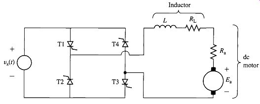
FIG. 56 Dc motor driven from a full-wave, phase-controlled rectifier.
Problem 13.
15. A three-phase diode bridge is supplied by a three-phase autotransformer such that the line-to-line input voltage to the bridge can be varied from zero to 230 V. The output of the bridge is connected to the shunt field winding of a dc motor. The resistance of this winding is 158 ~. The autotransformer is adjusted to produce a field current of 1.75 A. Calculate the rms output voltage of the autotransformer.
16. A dc-motor shunt field winding of resistance 210 ~2 is to be supplied from a 220-V rms, 50-Hz, three-phase source through a three-phase, phase-controlled rectifier. Calculate the delay angle Otd which will result in a field current of 1.1 A.
17. A superconducting magnet has an inductance of 4.9 H, a resistance of 3.6 m~, and a rated operating current of 80 A. It will be supplied from a 15-V rms, three-phase source through a three-phase, phase-controlled bridge. It is desired to "charge" the magnet at a constant rate to achieve rated current in 25 seconds.
a. Calculate the firing-delay angle O~d required to achieve this objective.
b. Calculate the firing-delay angle required to maintain a constant current of 80 A.
18. A voltage-source H-bridge inverter is used to produce the stepped waveform v(t) shown in FIG. 57. For V0 = 50 V, T = 10 msec and D -0.3:
a. Using Fourier analysis, find the amplitude of the fundamental time harmonic component of v(t).
b. Use the MATLAB 'fit()' function to find the amplitudes of the first 10 time harmonics of v(t).
19. Consider the stepped voltage waveform of Problem 18 and FIG. 57.
a. Using Fourier analysis, find the value of D (0 < D _< 0.5) such that the amplitude of the third-harmonic component of the voltage waveform is zero.
FIG. 57 Stepped voltage waveform for Problem 18.
FIG. 58 Stepped current waveform for Problem 20.
b. Use the MATLAB 'fit()' function to find the amplitudes of the first 10 time harmonics of the resulting waveform.
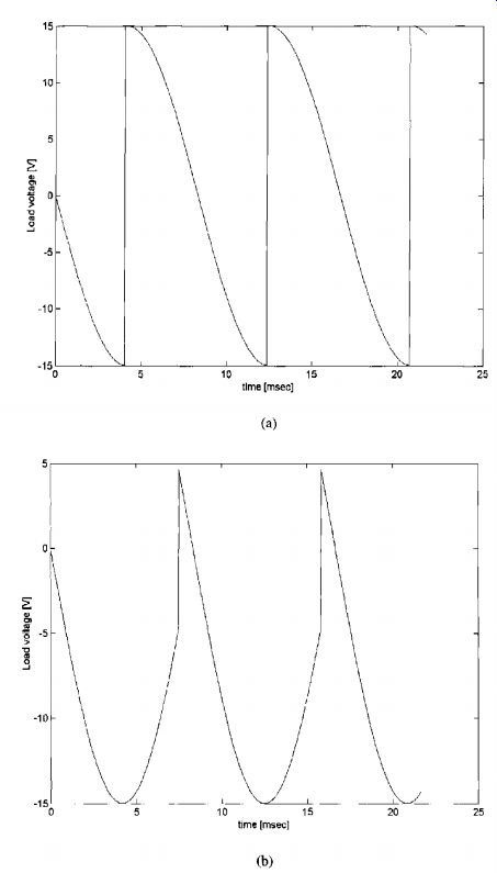
20. Consider Example 12 in which a current-source inverter is driving a load consisting of a sinusoidal voltage. The inverter is controlled to produce the stepped current waveform shown in FIG. 58.
a. Create a table showing the switching sequence required to produce the specified waveform and the time period during which each switch is either ON or OFF.
b. Express the fundamental component of the current waveform in the form il(t) = ll cos (cot + ¢1)
where 11 and t~l are functions of I0, D and the delay angle a d.
c. Derive an expression for the time-averaged power delivered to the voltage source rE(t) -Va cos ogt.
21. A PWM inverter such as that of FIG. 45 is operating from a dc voltage of 75 V and driving a load with L = 53 mH and R = 1.7 ohm. For a switching frequency of 1500 Hz, calculate the average load current, the minimum and maximum current, and the current ripple for a duty cycle D = 0.7.