AMAZON multi-meters discounts AMAZON oscilloscope discounts
... << cont from part 2a
Inductors and transformers
Transformers
'Inductance' is a property possessed by all conductors, and is related to their ability to generate a surrounding magnetic field when current passes through them. This property has a value, expressed in 'henries' (or milli or micro-henries), which is proportional to their length. However, the inductance of a conductor is increased if it’s wound into a coil, and has a maximum value, for a single layer coil, when the diameter of the coil is about five times its length.
If two, or more, coils are placed so that their magnetic fields interact, the passage of a current through one of them will induce a voltage across the other. This arrangement is called a 'transformer', and the efficiency of transformation is dependent upon the completeness of interaction of their associated magnetic fields. This is increased if the coils are wound around a ferro-magnetic core, which lessens the possible loss of magnetic coupling between any one winding and another.
Such a core material will also increase the inductance of the windings, and the extent to which the inductance of the windings is increased by the magnetic characteristics of the core is referred to as its 'permeability' (µ) and is measured on a scale in which a vacuum (or, for all practical purposes, air) is defined as having a value of unity.
The inductance, 'L', of a coil, wound around some magnetizable core, can be calculated from the formula:
...where N = number of turns, a = effective cross sectional area of core in cm^2 , / = effective length of magnetic circuit in cm., and µ=effective permeability.
Unfortunately, all magnetic core materials introduce some energy losses into the system due to 'hysteresis' and 'eddy current' effects. These losses will increase with operating frequency, and are due respectively to the internal energy absorption within the crystalline or molecular structure of the material on each reversal of its magnetization, and to the flow of current within the core material itself, constituting a multiplicity of un desirable short-circuited secondary windings.
For low frequency use, as in mains frequency power transformers, eddy current losses can be made adequately small by making the core from a large number of thin 'laminations', typically 0.2 - 0.4mm thick, with one surface coated with some insulating material, and which are stamped out in suitable shapes, as in FIG. 32, to allow a stack of laminations to be built up to fit the former on which the coils are to be wound.
FIG. 32 Laminated core assembly in transformers
At higher frequencies, the possible path length of eddy currents within the core material must be reduced still further, and typical core materials are formed, either from a mixture of magnetic materials and a thermosetting resin binder, in powder form - of which the simplest kind of magnetic material is just is very finely divided iron powder - known as 'iron dust' cores, or from some intrinsically non-conducting material such as a magnetizable ceramic, known as a 'ferrite', molded into the required shape.
Most of the ferrites are ineffective beyond about 2MHz, though a few formulations can be used beyond this frequency. For use at very high frequencies, as in radio or radar systems, air-cored inductors, or structures having the same effect, are normally used, to avoid the core losses introduced by higher permeability materials.
The permeabilities of a range of magnetic materials used for transformer and inductor cores are listed in Table 4.
Table 4 Permeabilities of transformer and inductor core materials
Material Permeability* Saturation flux density (Gauss)
Grain oriented 1000-8000 19,700 silicon steel (2-5% silicon)
Ferrites 2000-5000 2,500 (Fe.Fe2Ü4)
Nickel steel 5,000-20,000 8,000 (82% Ni, 2.0% Mo)
'Permalloy' 20,000-100,000 8,700 (79% Ni, 0.3% Mn)
'Mu-metal' 20,000-150,000 6,500 (75% Ni, 18% Fe, 2% Cr, 5% Cu)
'Sendusf 50,000 c. 7,000 (85% Fe, 10%Si,5%AI)
* Value will depend on method of manufacture and on operating flux density
Two things should be noted in relation to this table -- that, in general, magnetic alloys which have been designed to give high values of permeability will only allow somewhat lower levels of maximum flux density, and that the actual permeability of a core material will depend on the magnetic flux within it, and will normally increase with increasing flux density -- as the magnetic field aligns the magnetic dipoles within the material - up to some saturation value, beyond which the permeability will fall rapidly to a much lower value, as shown in FIG. 33.
It’s important to remember that this effect can occur in any circumstances where there is a DC current flow.
Permeability (m)
10K - 1K-I 100 10 "G 100 1k 10k
Flux density (B)
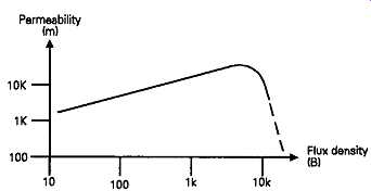
FIG. 33 Typical relationship between permeability and flux density in silicon
steel core material through a coil winding on a ferromagnetic core, as, for
example, in the use of an LF choke in a choke-capacitor filter smoothing circuit
in a DC power supply, where the flux saturation of the core, due to this current,
may substantially reduce the inductance of the choke.
This characteristic is used, deliberately, in 'magnetic amplifiers' where the use of a relatively small DC current, through a third winding on the core, is used to control a much larger output current from a power transformer.
The core losses of a power transformer will depend on the core flux densities used, and will increase rapidly as the flux saturation level is approached. In practical terms, for any given operating frequency, this means that there will be an optimum maximum flux density, which increases as the number of 'turns per volt' is reduced, for any given core material and cross sectional area.
This is expressed in the equation:
M_ £xl0 8 2S3SßA w
…where N is the number of primary turns, E is the applied voltage (RMS),/is the operating frequency, B is the maximum flux density, and A is the cross sectional area of the core in cm^2 . A fuller treatment of this subject is given by Builder, Hansen, and Langford-Smith in the Radio Designers Handbook, 4th edition, Section 5.
Grain-oriented silicon steel, in which the crystal structure is oriented during manufacture by cold rolling and annealing, (which also substantially increases its permeability in the direction of crystal alignment), is the most common material used for the cores of LF power transformers and chokes, because of its relatively low cost, and its high possible saturation flux density.
Improvements in LF transformer performance have mainly been obtained by better forms of core construction, to reduce flux leakage, and winding insulation, to allow higher operating temperatures, rather than by the use of more exotic core materials.
Mains power transformers, and other transformers intended for use at relatively low frequencies - say up to 10kHz - are normally made by winding the 'primary' (power input) and 'secondary' (power output) coils on a shaped insulating former within which the core laminations can be stacked, and interleaved to minimize the extent of the inevitable air gaps between the abutting lamination sections.
Typical lamination forms are shown in FIGs. 32a and 32b, known as 'E's and Ts, or 'T's and 'U's from their shapes. ('E's and Ts are the more commonly found types.) These are assembled into a rectangular stack of the kind shown in FIG. 32c, and a former of the type shown in FIG. 32d is made to hold the windings and to fit neatly around the core stack.
Core systems having a better efficiency, mainly in terms of their reduced external magnetic field and higher power handling capability for the same weight of core material, are the 'C core and 'toroidal' core forms shown in FIGs. 34a and 34b. In both these forms, the core is made by winding a continuous strip of thin lamination material, insulated on one or both faces to prevent eddy currents, into a 'toroidal' or doughnut shape, which is then totally impregnated with some synthetic resin to hold it in the required form.
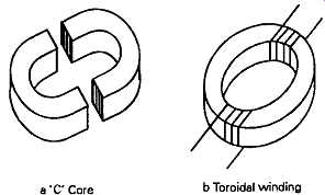
FIG. 34 --- Toroidal winding , *C Core D
In the C core structure, the core block is then sawn into two segments, and the opposing faces are ground flat so that when the two halves of the core are fitted together the residual air gap will be very small. A steel band is then usually fitted round the core, after the two halves have been inserted into the wound former, to clamp the two halves firmly together.
This type of core has now largely been supplanted by the toroidal construction, shown schematically in FIG. 34b, in which the core is left as a complete toroid and the primary and secondary windings are wound within and around it by a specially designed coil winding machine.
Though more costly than the conventional stacked lamination type of transformer, this construction offers the advantage of a very low external magnetic field, which makes it very popular for use in audio amplifiers, where a very low background 'hum' level is a desirable quality.
A useful adaptation of the toroidal type of transformer is the variable transformer, commonly known by the trade name 'Variac'. This takes the form of a cylindrical core on which a single-layer winding has been formed, with the insulating varnish removed from the face of the exposed windings at one end of the core.
An electrical contact is then made to the exposed part of the winding by means of a sliding graphite contact, mounted from a spindle rotated about the central axis of the core. Since the system behaves as an auto-transformer (i.e. one in which a section of the primary winding acts as a secondary), an adjustable proportion of the voltage applied to the primary winding can be tapped of f by the sliding contact.
Since one of the possible advantages offered by the use of a multiple winding transformer is that power may be transferred from one circuit to another, while retaining electrical isolation between them, care is taken to ensure that the windings are adequately insulated from one another and from the core.
Sometimes, in high quality units, this is done by dividing up the former, of the type shown in FIG. 32d, into smaller, separate, isolated sections, but this method of construction may somewhat lessen the electrical efficiency of the transformer by reducing the magnetic coupling. So, more usually, this inter-winding insulation is done by just inserting a layer of flexible insulating material between the windings.
If circuit requirements demand a particularly high degree of magnetic coupling between the windings, the primary and secondary windings may be wound as 'bi-filar' (or 'tri-filar') types, where two (or three) wires are wound simultaneously onto the core. In this case, the inter-winding DC isolation relies solely on the effectiveness of the insulating lacquer coating on the wires.
Electrostatic isolation between the windings can be achieved by the use of an 'electrostatic' or 'Faraday' screen. This is a sheet of electrically conducting foil, of copper or aluminum, insulated on both sides, and wound around the primary winding to give slightly more than a complete single (open circuit) turn, before the secondary winding is applied. A connecting lead, from the electrostatic screen, is led out from within the windings so that it can be taken to an electrical 'earth' point.
For higher frequency use, in low power audio transformers, as, for example, in line matching or as microphone step-up transformers, conventional E and I type laminations are most commonly used, made from 'Mu-metal' or one of the other high permeability, and high cost, Nickel-Iron alloys. These laminations may often be very thin, down to some 0.1mm in thickness, to minimize core losses.
Depending on their intended applications, power transformers are made either in open form, with the windings insulated, but otherwise exposed, or in screened forms, with an external metal case surrounding the transformer. However, such a case won’t provide electromagnetic screening unless it’s made from some ferro-magnetic material.
Circuit diagram symbols for a simple two-winding transformer, a transformer having an internal electrostatic screen, a transformer with a dust-iron core, and a variable transformer, are shown in FIG. 35. How ever, as with other components, the actual equivalent circuit of a simple two-winding transformer is more complex, as shown in FIG. 36.
In this, Lyp is the primary leakage inductance, Rp is the primary winding resistance, Cp is the lumped primary inter-winding capacitance, ?p represents the primary core losses, L is the primary winding inductance,/^ is the secondary winding inductance, Rs is the secondary winding resistance and Lls is the secondary leakage inductance.
The practical significance of these spurious effects is examined in Sections 11 and 15.
Electrostatically screened type
Dust iron; Variable cored RF transformer
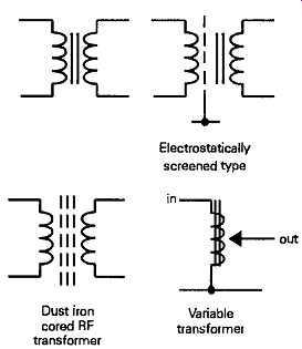
FIG. 35 Circuit symbols for transformer types
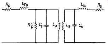
FIG. 36 Spurious electrical components within normal two-winding transformer
Inductors
The inductor is potentially a versatile component in electronic circuit design, but has not been used widely in such applications because it has not been possible, until comparatively recently, to buy, of f the shelf, small inductors, having precisely defined values, in as wide a range of values as, for example, wirewound resistors.
The method of construction employed depends upon the inductance value required and upon its intended operating frequency range. Components having inductance values in the range 2-100 henries (H), intended for use in power supplies to smooth out AC 'ripple' from the supply line, in conjunction with a 'smoothing' capacitor, are generally built in a similar manner to a normal mains power transformer, with a multiple layer winding built up inside a molded former, enclosing a laminated iron alloy core, of the general form shown in FIG. 32d.
The impedance of an inductor, for which the circuit symbol is shown in FIG. 37, increases with frequency in a manner defined by the equation
ZL = 2nfl. (6)
… and this characteristic allows it to be used, in AC applications, to perform the function of a resistor, in generating a voltage drop proportional to the (ac) current flow through it.
FIG. 37
However, it also has the valuable characteristic that, since its impedance is dependent on frequency, net works combining inductors with resistors and capacitors can be used for frequency selective applications, such as filters, or tuned circuits, capable of generating either very high or very low impedance paths at some selected frequency.
Small inductors, intended for low signal-level circuit applications, in the inductance range from a fraction of a micro-henry to some hundreds of millihenries, are most commonly made by winding a coil of insulated copper wire upon some rigid insulating former, of ceramic or hard thermoplastic, typically in rod form, to which solderable connecting leads are attached.
It’s unusual for such small inductors to employ a magnetic core material, since this would restrict the frequency range over which they could be used, and this, in turn, limits the maximum inductance range which can be provided in a physically small component. Small inductors of this type are often coated with an opaque lacquer, and color-coded like resistors to show their inductance in micro-henries.
Connectors and switches
Contact erosion and contamination
The requirements for both of these types of component are basically similar, in that they are needed to join parts of the electrical circuit together with as low a level of contact resistance as possible. Unfortunately, all metallic surfaces exposed to air will ultimately become contaminated with deposited films of grease or dirt, and will oxidize or corrode because of chemical reactions with atmospheric oxygen or other corrosive gases.
If the contacting surfaces are arranged to slide together, this action will help to scrape the contacts clean, but with the penalty that the greater the contact pressure, the more effort will be required to bring them together and the greater the mechanical wear on the contacts. In both switches and connectors it’s good design practice for the component to be constructed to restrict the access of air, to try to preserve contact cleanliness.
Silver is the preferred metal for most plug-socket connectors and switch contacts, in that corrosion processes will normally only form a thin, and partially conducting, layer of silver oxide or sulphide. Thermal diffusion processes will then cause this to be 'doped' with silver atoms in the same manner as occurs in semiconductor junctions, which greatly increases its conductivity. A small 'wetting' current may also be helpful in keeping the contact resistance low, though there may then be some small erosion of the negatively charged contact.
The plating of silver contacts with a thin layer of gold, which is helpful in prolonging the life of sliding contacts, may actually worsen the contact resistance, if silver sulphide growths spread through the minor cracks in the gold surface layer, since the presence of the gold layer may prevent the silver doping effect.
Also, when arcing may occur during the switching of higher power circuits, silver has a better resistance to arc damage than gold, though, if cost is no object, palladium-nickel alloy (85% Pd, 15% Ni) contacts are very arc resistant, and platinum is even better. The presence of atmospheric oxygen helps to lessen arc induced contact erosion. However, both palladium and platinum suffer from the snag that local surface catalytic action can cause the formation of 'brown powder' - an adhesive non-conducting dust produced by the polymerization of organic gases and other contaminants present in the atmosphere.
At present, the best switch/connector contact construction for low contact resistance is probably gold plated Pd/Ni alloy, since the gold layer acts as a lubricant, and tests have shown such contacts to retain a very low contact resistance, of the order of 2-3 milliohms, after 25,000 operation cycles.
The properties of electrically useful metals and some of the more commonly used contact alloys are listed in Table 5.
In general, materials with high melting points will give good arc resistance, and mechanical hardness will assist in prolonging contact life. Alloying almost in variably lowers both melting point and conductivity, but is used where some combination of physical properties is best obtained by this means.
Since the mechanical components of any electronic system are now by far the least reliable, and most trouble prone, part of the equipment, it’s preferable to use the most robust and best made plug/socket connectors that physical space or considerations of cost will allow. This advice is even more appropriate to switches, since the area of physical contact is likely to be much smaller.
===
Table 5 Properties of switch and connector contact metals
Material Silver; Silver with 0.15% Nickel Silver with 15% CdO Gold Copper Palladium with 40% Silver Nickel Palladium Platinum Rhodium Indium Molybdenum Tungsten Melting point (°C) 961 960 961 1063 1083 1200 1453 1552 1769 1966 2454 2610 3400
Relative hardness
80 100 (ref.) 125 60 100 100 200 100 95 130 220 250 450
Conductivity (mho/meter)
62 58 42 44 58 2.4 14 9.0 9.5 22 19 19 18
===
Switches
These are made in a wide range of styles, for different types of circuit or mechanical applications. Most of the types and descriptions offered are self-explanatory, so little guidance is necessary. However, some points are worth watching.
Rotary switches
These are used as small current wafer switches, and also as higher power stud-type switches. In both of these forms, one contact of the switch is taken to a movable wiper which slides over the other fixed contacts. The wafer switches used largely in small-signal electronics circuitry are offered in three basic switching styles, 'break before make', 'make before break', and 'shorting' types. Their manner of operation is shown schematically in FIG. 38.
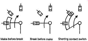
FIG. 38 --- Make before break
Break before make; Shorting contact switch
A mechanical indent mechanism, usually provided by a spring- loaded ball riding over a notched pathway, locates the rotor at the correct switching positions for the moving contact to register with one or other of the fixed ones. Although there is no specific limit on the range of switching positions, the most common number is twelve, allowing choices, within the range, of 1-pole 12-way, 2-pole 6-way, 3-pole 4-way, 4-pole 3- way and 6-pole 2-way.
The so-called 'miniature' wafer switch, having just a single 12-contact switch section, is an attractive option because of its compact construction and low cost. These switches, however, almost always rely on a single sliding contact, of the kind shown in FIG. 39a, which is very much less reliable in use than the twin-wiper type of contact, shown in FIG. 39b, which is almost invariably used in those wafer switches which allow multiple gangs of wafers to be assembled along the same actuating spindle.
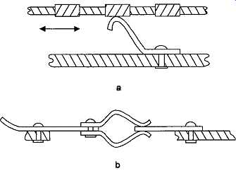
FIG. 39 Wafer switch constructional forms
The thumb-wheel actuated edge switches employ similar constructional forms, and the same comments apply. However, these switches, and the miniature printed circuit board mounting DIL (dual in line) switches are seldom required to perform very many operations during their service life, and don’t there fore wear as much as front panel operated units.
Because it’s very difficult to exclude the ambient atmosphere from such switches they will inevitably suffer from atmospheric contamination and corrosion.
Because of their slow break action, they are unsatisfactory for switching power circuits.
A version of the wafer switch, but assembled on a linear wafer, is used as a small-signal push-button switch. These are particularly valuable in the form in which they latch in position, and where they can be grouped in banks so that the actuation of any one switch of the bank will release the others.
Toggle switches
These are particularly appropriate for switching power supply circuits, because of their rapid make/break action, which minimizes contact damage due to arcing. Such switches will usually be sold with a specific current/voltage rating, which will be for use with AC circuits. Their DC rating will be considerably lower, because arcs may continue for a longer period after the switch contact is broken - especially on inductive loads.
Standard panel mounting toggle switches are avail able in single, double, triple or quadruple pole forms, in either single or double throw, usually referred to as 'SPST', 'DPDT' and so on. They may also be offered in spring-biased forms, where the toggle will normally return to one or other position when it’s released.
Center (Off position) biasing is also commonly available.
The 'microswitch' is a particular version of a 'rapid make-break' toggle switch, based on an internal beryllium/copper leaf spring, which will trip over from one state to another on a very small movement of the actuating button. These are commonly just make break types, but change-over forms are available.
They can offer very long life expectancies, up to 10^7 operations.
Keyboard switches
These are becoming increasingly widely used because of the spread of calculators, computers, and other similar systems. The main requirements here are for very long life, small size and resistance to the ingress of dust or liquid spillages. Since contact resistance is often not very important, because they will mainly be used to operate very high impedance circuitry, they may simply employ conductive rubber diaphragms, pressed by the key button into contact with one or more conductive tracks on a substrate.
In higher quality equipment, miniaturized toggle switches, based on the microswitch type of mechanism, are more common, because the toggle action gives a better keyboard 'feel'.
Relays
This is the term used to describe the whole class of remotely actuated switches, usually electromagnetically operated. In their classic form, they will have the general type of construction shown in FIG. 40, in which an electro-magnet is arranged so that, when it’s energized, it will pull down a spring-loaded rocker arm, which will push a movable contact away from its rest position so that it comes into connection with another contact.
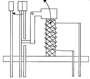
FIG. 40 Mechanical toggle relay
This can give either a single 'make', or a 'change over' action, and there can be as many such switch sections as required, though four such parallel switches is commonly the maximum available in commercial units.
Since the system can be completely sealed against the ambient atmosphere and other airborne contaminants, good contact life and system reliability is easily obtained, especially on low power circuitry, where contact arcing does not occur.
The major snags of such devices are that contact 'bounce' or 'chatter' will nearly always occur to a minor extent and that the intrusion of the electrical switching spikes, when the coil is energized or de energized, into low signal level circuitry connected to the relay contacts, is difficult to prevent completely, particularly since the mechanical design of the relay does not normally include any screening between the energizing coil and the actuated contacts.
In addition to the recommended coil operating volt age and coil resistance, the makers will usually also quote the 'pull-in' and 'drop-out' voltages for the relay, and sometimes also the speed of operation, in milli or microseconds, for a given operating voltage.
In order to avoid problems when such relays are operated from solid state circuitry, it’s customary practice to connect a small power diode across the coil, as shown in FIG. 41, to 'snub' the switch-off voltage spike which would otherwise occur.
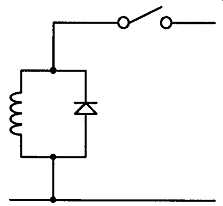
FIG. 41 Conventional diode snubber circuit used with relay switching.
A particularly useful type of relay, where high switching speeds and long life expectancy, (up to 10^8 operations), are essential, is the reed relay. This has the form shown in FIG. 42, and consists of a thin 'reed' of gold-plated nickel or iron, which can be pulled into contact with another such reed when an axial magnetic field is applied, either by some external permanent magnet being moved into proximity to the reed, or by causing current to flow through a coil (sometimes called a 'solenoid') wound around the tube which holds the reed.
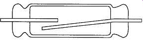
FIG. 42 Construction of encapsulated reed relay.
These reed switches are generally sealed inside a thin glass tube containing some inert gas -- a vacuum is not used because it would encourage cold welding of the contacts -- and are most commonly available as single 'make' or 'change-over' versions. Although not specifically aimed at power switching, reed relays can switch currents of up to 2 amperes.
A convenient modern form of this relay is that in which the whole assembly of reed switch and opera ting coil is molded into a small plastics block, having a physical size, and connecting pin layout, which allows it to be plugged into a standard 14-pin dual-in line integrated circuit holder.
A form of reed relay which has both a low contact resistance and high freedom from contact bounce is the 'mercury wetted' relay, in which the contacting reeds are nickel plated and grooved to assist the flow, by capillary action, of mercury from a small pool at the base of the reed, as shown in FIG. 43. How ever, this requires that the reed element shall be mounted vertically to prevent inadvertent shorting of the contacts by the mercury globule.
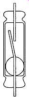
FIG. 43 Mercury wetted reed relay
A similar mechanism is employed in the mercury 'tilt switch', where the capsule is constructed so that the switch can be opened or closed by alteration of its positional angle.
Housings
All electronic systems will require some form of en closure or housing, to present a neat finished appearance to the unit, to protect the internal components from damage, and to protect the user from possible electrical shock, especially when the equipment is mains voltage operated.
The housing can also serve a number of other useful functions, in assisting in the removal of heat from internal components by conduction from the component, if the housing is made from some thermally conductive material, and in protecting possibly vulnerable components from atmospheric dust, contamination or corrosion. Ventilation of the housing to help keep the circuit components cool may cause problems by increasing the accumulation of airborne dust and grease, so these aspects should be considered in the choice of enclosure.
In very low signal circuitry, or in designs which operate at a high impedance level, the enclosure will normally need to provide some electrical screening for the circuit to prevent the pick up of electrical noise or 'hum' from the surroundings - generally referred to as EMI (electromagnetic interference) - which would worsen the no-signal background noise level of the equipment.
Similar considerations apply, in reverse, if the circuit generates electrical signals, such as high frequency oscillatory voltages, which could cause interference in adjacent equipment. This is particularly the case in radio frequency designs employing local oscillators, and in 'switch-mode' power supplies.
Where electrical screening must offer a high degree of environmental isolation, signal and power supply ports through the metal screening enclosure may re quire specially designed feed-through insulators, usually combined with a ceramic decoupling capacitor to lessen the extent of RF transmission along the connecting leads.
A particular application in which the design of the enclosure is very important is found in industrial electronics installations where the equipment is to be used in a corrosive, or flame- or explosion-hazard environment. In the latter cases, the equipment may require to be filled with some inert gas, maintained at a positive internal pressure, to ensure that the electrical circuit is never allowed to come into contact with the hazardous environment.
An alternative approach is that defined by the inter national standards defined in IEC 79-10, BS5501/BS5545 or CENELEC standard EN50-020, in which it’s required that the equipment should be designed so that the maximum electrical energy avail able within the circuitry is below the level at which any spark or thermal effect is capable of initiating a flame or explosion.