AMAZON multi-meters discounts AMAZON oscilloscope discounts
Relays
These are a special category of switches, in which the mechanical operation of the switch arm is performed by an electromagnetic actuator driven by a wound coil.
Showing the coil in physical proximity to the switch mechanism, as illustrated in FIG. 8h- which might depict a 'reed' relay, with an air-cored operating coil - tends to clutter up the circuit diagram, so it’s more common to separate these, as shown in FIG. 8j.
The relay operating coil can then be drawn as a simple box, on which, for example, the legend 'RL1' -- denotes that relay No. 1 has two operating
FIG. 8 switch contacts. This then allows the switch elements which are operated by this relay to be placed anywhere convenient in the circuit drawing, and labeled 'RLi G and 'RLi-2' to show how they are operated.
It’s good practice to append 'nc' or 'no' signs against such relay switch contacts to show they are 'normally open' or 'normally closed' - when the relay operating coil is unenergized.
Transistors and diodes
The normal semiconductor junction diode is represented by one or other of the equivalent forms shown in Figs 9a or 9b. No specific notation is used to distinguish between a low-power, 'small signal', diode and a high-power rectifier device, so the engineer must infer this distinction from the part of the circuit in which the device is placed.
'Bridge' rectifiers, or a group of diodes arranged to form a full-wave rectifying block, are conventionally shown as in FIG. 9c. However, the diode symbols are sometimes omitted from the drawing entirely, giving the picture shown in FIG. 9d, which relies for its interpretation on the presence of the'+','-' and'-' (AC input) signs at the corners of the diagonal square.
This may be simplified even further to the symbol of FIG. 9e, in which a diode is shown within the square, and even the '+','- ' and '- ' symbols are left out.
'Zener' or voltage regulator diodes are denoted by the symbols of FIG. 9f or 9g. A similar symbol is sometimes used to denote a 'hot-carrier' or 'Schottky' type of point contact diode. A preferred symbol for this device is shown in FIG. 9h.
Normal NPN junction transistors are drawn as shown in FIGs. 9j - .9m, according to the preference of the draughtsman. Enclosing the transistor symbol with a ring, to indicate the physical boundary of the device, as in FIG. 9m, allows the envelope to be extended, as for example in FIG. 9n, to denote a dual or multiple device mounted within the same housing. Such a symbol probably implies that both devices are fabricated on the same chip, so that both sections will have closely similar operating characteristics.
In both NPN and PNP junction transistors, the emitter lead is denoted by the line with the arrow head; pointing towards the 'base' in the case of a PNP device, and away from it in the case of the NPN version. The angled line without the arrow head denotes the collector junction. The line joining at a 'T' refers to the base of the transistor. Symbols for PNP junction transistors are depicted in FIGs. 9p, 9r and 9s.
The line or bar denoting the base area of the transistor should be blocked in. Where this is left as an open rectangle, as in FIG. 9t , it’s usually taken to mean that the device is of the 'super-Beta' type, having a very high current gain but a very low collector-emitter or base-emitter breakdown voltage. These types of transistor are normally only found in integrated circuits.
The drawings shown in FIGs. 9u or 9v are sometimes found as a representation of a junction transistor. This is a more logical analogy for the de vices now made than the symbols of Figs 9j or 9p - which typified the early, and now obsolete, point contact devices. However, this more accurate symbol has never been widely adopted, and remains a some what eccentric variation.
Field effect devices
These exist as junction types, and as 'MOSFET' or 'insulated gate' (static charge operated) field effect devices. The symbols used to represent junction FETs are as shown in FIGs. 10a and 10b, which denote 'N-channel' and 'P-channel' devices respectively, shown in FIGs. 10c. If these devices are truly symmetrical, so that 'drain' and 'source' connections are interchangeable, the gate junction will be shown centrally, as in FIGs. 10c and 10d.
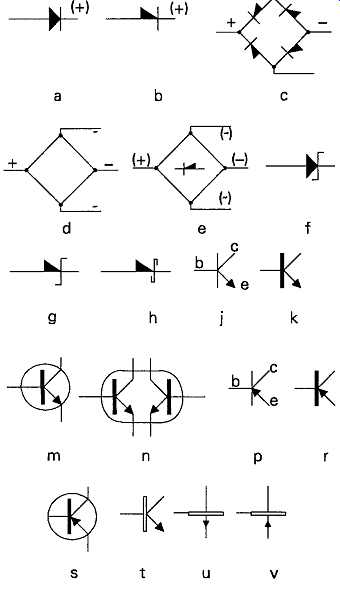
FIG. 9
Insulated gate devices are shown by the symbols of FIGs. 10e, (N-ch) and 10f, (P-ch). The distinction between an N-channel MOSFET and a P-channel one is denoted by whether the substrate junction con tact has an arrow head facing towards or away from the substrate bar symbol.
Sometimes the insulated gate symbol is drawn with the connection at the opposite end of the gate region, as shown in FIG. 10g, (P-ch), to make this distinction somewhat clearer. MOSFET devices are also available with dual gate regions as shown in FIG. 10h.
These devices exist in two types, the 'depletion' and 'enhancement' mode forms, distinguished by whether the source/drain channel is normally conducting or whether some forward bias must be applied to the gate to cause conduction. While the 'MOSFET' symbols shown in FIGs. 10e - 10h will often be used interchangeably for both of these forms, the drawings of FIGs. 10j and 10k, where there are gaps in the channel symbol, may sometimes be used specifically to denote 'enhancement' style devices.
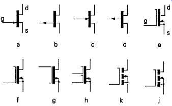
FIG. 10 Thyristors and triacs
There are a wide range of these specialized current control elements, with a correspondingly wide variety of circuit symbols. Of these the most common are thyristors, also known as silicon controlled rectifiers, and triacs, which are a bi-directional form of thyristor.
A modified diode symbol is used to represent these devices, as shown respectively in FIGs. 11a and 11b. The device denoted by the symbol of FIG. 11c is effectively identical in characteristics to the thyristor, but is known as a programmable unijunction transistor.
The device shown in FIG. 11d is a silicon con trolled switch, and those of FIGs. 11e and 11f are different forms of 'diac' or bi-directional trigger de vice. The final commonly found member of this family is the unijunction transistor denoted by FIG. 11g.
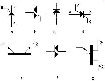
FIG. 11
Thermionic valves and other vacuum envelope devices
These are also based on representations of the components they depict, with directly heated (filament type) and indirectly heated cathodes drawn as shown in FIGs. 12a and 12b. Grids are depicted either as dotted lines or as a continuous horizontal zigzag, interposed between the cathode and the anode, and 'plates' or anodes are shown as rectangular boxes or 'T' shaped symbols, again depending on whether the USA or European convention is used.
For example, in the European style of drawing, a directly heated diode valve would be shown as in FIG. 12c, while an indirectly heated triode would be shown as in FIG. 12d. The number of electrodes within the valve - ignoring the heater of an indirectly heated type - is categorized by adding the suffix '-ode' to a prefix based on the classic Greek numerical sys tem, so that a diode means a two electrode valve, a triode means one with three electrodes, and so on with tetrodes, pentodes, hexodes and heptodes, illustrated in FIGs. 12e- 12h.
Exceptions are sometimes made to this rule by ignoring the presence of the beam confining plates of the valve shown in FIG. 12j, which is still classed as a beam-tetrode. Note also that the third or 'suppressor' grid of a pentode, or the beam confining plates of a beam-tetrode, may frequently be internally connected to the cathode. This connection may not always be shown in the circuit symbol.
Combination valves, such as double diode triodes and triode hexodes, are also made. Symbols for these are shown in FIGs. 12k and 12m. A valve type which has not been superseded is the cathode ray tube.
In this, the electron beam can be focused and deflected either electromagnetically, by means of externally mounted coils, or electrostatically, by the use of internal electrode structures. These differing types give rise to the two different symbols shown in FIGs. 12n and 12p.
Some 'cold cathode' or gas-filled valves were made, such as the 0Z4 rectifier or the 0A3 series of voltage stabilizer tubes, shown in FIGs. 12q and 12r. In these the presence of a deliberately introduced gas filling is sometimes, but not invariably, denoted by the insertion of a small dot within the envelope symbol.
Some ambiguity exists in the representation of the stabilizer valve, shown in FIG. 12r, in that this is sometimes drawn inverted, as in FIG. 12s, with the curved plate as the cathode - since this reflects more truly the actual structure of the component.
Valve symbols for indirectly heated valves are quite frequently drawn with a conventionally shaped cathode, but without showing the heater element at all, as in FIG. 12t. This omission should not be taken to imply that these are gas filled or cold- cathode devices.
Linear integrated circuits (ICs)
There is an enormous and growing range of these components, of which most will be depicted in a circuit diagram simply as a rectangular box carrying some descriptive label, or perhaps just a type number.
A few, however, have become sufficiently widely used that they have acquired their own distinctive symbols.
Of these the most common is the Operational amplifier' IC gain block, shown in FIG. 13a.
This is normally shown as a triangle, with two inputs on the vertical face, and an output at its vertex. The 'non-inverting' and 'inverting' inputs are indicated by '+' and '-' signs attached to the inputs, within the triangular symbol. Most commonly, the presence of supply connections, from, for example, a pair of regulated +/-15V supply lines is simply assumed, and not shown at all.
Where these are shown, they may often merely be truncated lines terminated by V or '- ' signs, or by conventional symbols denoting these, as shown in FIG. 12 FIGs. 13b and 13c. Where an external control is used to adjust the output DC offset voltage of an opamp, this will be depicted as shown in FIG. 13d.
In some RF amplifier gain blocks a pair of anti-phase outputs may be provided. This is shown in FIG. 13e.
A special category of opamp. ICs, sometimes called 'Norton' amplifiers, is that in which a non inverting input is added to an inverting gain block by the use of an input inverting circuit, such as a current mirror. To distinguish this type of circuit from a true opamp, in which both of the inputs would have comparable input impedances and other characteristics, the symbol of FIG. 13f is used.
Voltage regulator ICs, though very widely used, are still just drawn as rectangular blocks, as in FIG. 13g. Constant current sources, used both within IC gain blocks, and available as separate ICs, are depicted by the equivalent symbols of FIGs. 13h, and 13j.
Current mirrors, or constant current sources whose output current is equal to, or is controlled by, some input reference current, are represented by FIG. 13k.
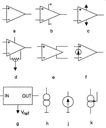
FIG. 13
Logic ICs
Though digital circuit functions are not within the scope of this book, these devices may often be used as parts of linear circuit designs, and a number of recognized symbols have evolved.
The diagram of FIG. 14a is that for a simple single-input buffer, with the input and output conventions the same as those for an operational amplifier, i.e. input on the vertical face of the triangular symbol and output at its apex. The small loop at the output point of FIG. 14b denotes phase inversion, so that this device would be an inverting buffer stage. The internal gain will usually be greater than unity, so these buffers can also be used as low performance linear amplifying stages.
The symbols shown in FIGs. 14c, 14d and 14e, are 'AND' gates, in which an output requires that appropriate signals are present at all inputs. Two, three and four input AND devices, of the type illustrated, are common. As before, the presence of a small loop on the output implies phase inversion, so that the device of FIG. 14f will be a 'two input NAND'. Similarly, a loop on an input connection, as shown in FIG. 14g, would imply a phase inversion of the input signal at this point.
The symbols shown in FIGs. 14h and 14j are two and three input OR' gates, and that of FIG. 14k is a two input 'NOR', by the same convention as above. In OR' gates, as the name implies, an output will be given if a signal is present at either input. A special case of the OR' gate is the 'exclusive OR', shown in FIG. 14m. This is a device in which an output will be given if a signal is present on either input, but not if it’s present on both.
Other logic ICs are usually represented by rectangular blocks, with appropriate symbol markings shown to indicate the connections.
As mentioned above, the DC supply connections to 'logic' ICs, which are typically as shown in FIG. 14n, are often omitted from the circuit drawing in the interests of simplicity.
Light operated and light emitting devices:
This type of function is depicted by the use of a pair of parallel arrows appended to the symbol. If light is emitted, the arrows will point away from the device, as in the light emitting diode of FIG. 15a. If light can modify the characteristics of the device, the arrows will be shown pointing inwards, as in the wide family of light sensitive or light actuated components such as the photo diode, photo transistor, photo resistor, or light actuated SCR shown in FIGs. 15b - 15e.
A different convention is adopted for heat sensitive devices, such as the thermistor, where this is shown by a dot alongside the resistor element as in FIG. 15f.
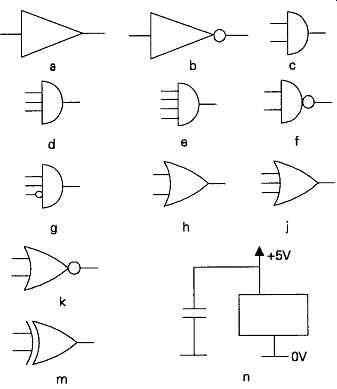
FIG. 14
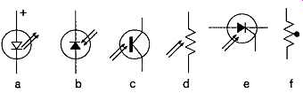
FIG. 15
Miscellaneous symbols A DC voltage source, such as a dry cell battery, is drawn as shown in FIGs. 16a and 16b, where FIG. 16a represents a single cell, or perhaps a notional low voltage source, and 16b a multiple cell battery, or a symbolic high voltage DC source. An AC source, of any potential, or an AC signal source, is denoted by FIG. 16c.
The normal drawing for a quartz crystal resonator is that of FIG. 16d or 1.16e. The former is preferable because of the possible confusion of the symbol of FIG. 16e with the Japanese symbol for an electrolytic capacitor. That for a 'surface acoustic wave' filter is as shown in FIG. 16f . Another common symbol, found in radio circuits, is that of FIG. 16g, which denotes a 'mixer' or 'modulator' stage. The symbol used in radio circuitry for the aerial connection is as shown in FIG. 16h, where this is a single wire type.
A 'dipole' aerial is shown in FIG. 16j.
A convenient shorthand way of representing circuit elements - such as a group of coils and capacitors, but possibly made up from other component types - which are used to remove a section of the signal frequency spectrum, known collectively as 'filters', is by the use of the symbols shown in FIGs. 16k, 16m, and 16n, or 16k', 16m' and 16n', which represent 'low-pass', 'bandpass' and 'high-pass' filters respectively.
The way in which a screened cable is represented is shown in FIG. 16p, and a coaxial or similar connector as shown in FIG. 16q. A 'jack' socket is shown in FIG. 16r.
Output devices such as headphones and moving-coil loudspeaker units are shown in FIG. 16s and FIG. 16t respectively. The normal symbol for a micro phone is as shown in FIG. 16u and that for a tape recorder 'pick-up', 'record' or 'erase' coil is as shown in FIG. 16v. The symbol used for a fuse is as shown in FIG. 16w.
Various drawings have been used to denote a filament lamp bulb, but I prefer that of FIG. 16x. A neon or similar gas discharge lamp is shown as in FIG. 16y, and a 'fluorescent' tube as in FIG. 16z. A current or voltage indicating meter is represented as in FIG. 16aa. Where this is part of a more elaborate instrument such as a milli-voltmeter or distortion meter, the meter symbol will be enclosed within an appropriately labeled box, as in FIG. 16ab.
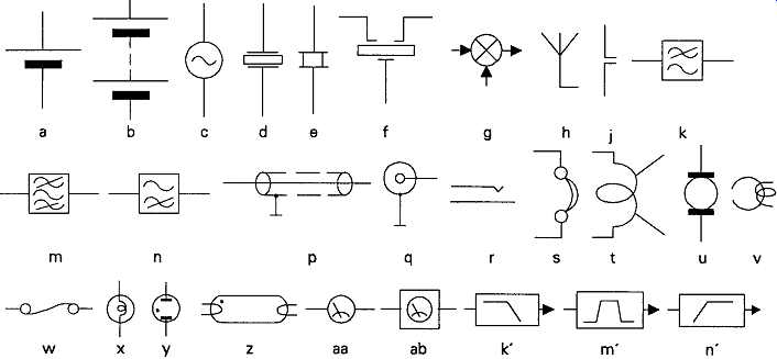
FIG. 16