AMAZON multi-meters discounts AMAZON oscilloscope discounts
Basic design philosophy
The purpose of a circuit drawing is to give a rapid visual explanation to the viewer of how the circuit works, and how the individual component parts relate to one another. Unfortunately, in practice, drawings are often made with the sole aims of showing the connections between the components in an accurate manner and of producing a neat looking final result.
Whether or not the actual interconnections are easy to follow, or how readily the engineer can discover the way the circuit operates, may not be a particularly high priority at the time the drawing is made.
Certain ground rules will help to keep the drawing simple in appearance and easy to follow. These are:
1. Adopt a consistent policy for the flow direction of signals, such as 'inputs' on the left-hand side of the drawing, moving across to 'outputs' on the right-hand side.
2. Keep positive supply lines at the top of the drawing, and negative supply lines, if present, at the bottom. Also, where polarity sensitive components are employed, try to position these so that the potential appearing across them has the same orientation as that of the supply lines. If there is an 'earth' or 0V line this should be positioned between the +ve and -ve lines.
3. Where the proliferation of supply lines will tend to confuse the picture, because of their frequent crossing of signal lines, use conventional symbols, as shown in FIG. 1, to indicate their destinations. The convention here is that FIG. 1a denotes a connection to a 0V supply line, which may or may not be connected to the chassis of the equipment, while that of FIG. 1b will indicate a direct connection to a metal chassis and Figures 1e or 1d will denote an earth connection.
The symbols of FIGs. 1e and 1f will imply a connection to the positive and negative supply lines. The drawing can frequently be greatly simplified by this technique, and if there are several different power supply or 0V return lines the appropriate ones can easily be indicated by numbers or letters.
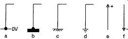
FIG. 1
4. Avoid groups of connections drawn as closely spaced bundles of parallel lines. Although these can give a drawing a tidy appearance, it’s very easy for the reader to lose track of the connection he is tracing through the circuit. It’s much better to use labels or supply sign conventions instead.
A comparative example is shown in FIGs. 2a and 2b, in which the latter drawing is not only simpler, and easier to follow, but actually gives more information about the operation of the circuit than FIG. 2a. In view of the complexity which can arise in showing the interconnections of just five components, it’s easy to see how confusing the circuit drawings for more complicated systems may become, unless some care is taken to make them easy to follow.
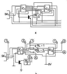
FIG. 2
Avoidance of ambiguities
The most common source of ambiguity in circuit diagrams concerns wiring connections which join, or which cross without joining. Several conventions exist in this area. Of these the most common is the use of a 'blob' on a junction of two wires, as shown in FIG. 3a, to distinguish this from a crossing without junction, shown in FIG. 3b.
Unfortunately, in printing or subsequent reproduction, spurious 'blobs' can appear because of ink accumulations where lines cross, giving a wrong indication of circuit function. To avoid this type of mistake, it’s good practice to make sure that junctions are never shown as simple crossings with 'blobs' but as staggered connections as shown in FIGs. 3c or 3d.
Alternatively, a loop can be inserted where lines cross without connection, as shown in FIG. 3e.
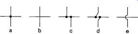
FIG. 3
RIAA stage Aux inputs Input buffer Rumble filter
Tone controls
The other major uncertainty arises where earth or W line connections are specified. Quite often the performance of the circuit depends critically upon the position of the 0V or earth line returns, and a simple connection to an earthed (grounded) chassis may not be acceptable. In this case the forms of connection should be distinguished from one another by the use of the symbols shown in FIG. 1, and where separate 0V or earth line returns are necessary these should be labeled numerically.
Conventional assumptions
Some conventions can cause difficulties to the inexperienced. One of these, as noted below, in FIG. 13a, in relation to operational amplifiers, is that these ICs are normally powered by stabilized +/-15V DC supply lines - unless otherwise specified - so it may be taken for granted that the IC will be connected to its appropriate supply lines without these connections being shown at all on the circuit diagram.
A similar convention is often assumed with logic ICs, which will usually be connected between the O V rail and a fixed +5V line. The existence of such a supply line is frequently taken for granted, and not shown in the circuit drawing, as is the presence of a small ceramic 'by-pass' capacitor, to decouple the supply to the 0V line at its point of connection to the IC, as shown in FIG. 14n. However, there may be exceptions to this rule, and the fact that no connections are shown may not always mean that a+5 V rail is used.
Block diagrams:
It’s often helpful when explaining the function of a relatively complex circuit - or group of circuits - to make use of 'block diagrams', in which the function of each block is described within its outlines, to show how the several parts of the circuit relate to one an other. An example based on an audio amplifier and preamplifier is shown in FIG. 4.
The specific circuit layout of the individual function blocks can then be shown separately at a later stage in the circuit description, when required.
Gain and balance controls
Power amplifier LS switching
Power output indicator | LS outputs
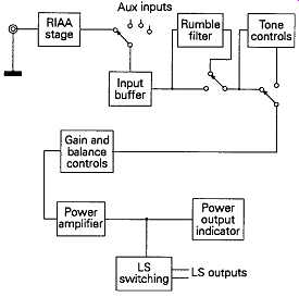
FIG. 4
The theoretical circuit
In addition to providing an illustration of the way in which the various components of the circuit relate to one another, and an indication of the flow of the signal path and the currents drawn from the power supply lines, the circuit diagram also allows the types and values of the separate components to be shown. It may also be helpful, as an aid to understanding of the circuit function, or subsequent fault diagnosis, if the nominal currents flowing in the various supply line paths are also indicated.
Although designers are traditionally assumed to set down their thoughts on the backs of envelopes, from which a fully-fledged design may spring into existence - and, indeed there may be designers who really do work like this - there is little doubt that the extra time spent, at the design stage, in producing a fully labeled circuit drawing, greatly facilitates the calculation of circuit performance, and allows thermal dissipations and other characteristics of the design to be assessed before the prototype is assembled.
Technical terms
As I explained in the preface, it’s my hope that this guide will be useful to engineers with little existing knowledge of electronics. To this end, I have tried to explain technical terms as they arise. However there are cases where this would make the text unduly lengthy, so, where I have omitted explanations, I would refer the reader to the section which deals with the component or technique in question.
Circuit symbols and useful conventions In the beginning, most of the circuit symbols, were simplified representations of the actual components themselves: such as that for a resistor being shown as a piece of resistive wire laid down in a zigzag path to increase its length, or a capacitor as a nominal pair of parallel conductive plates, in proximity to one another, but separated by an air gap, or a transformer being represented by two coils of wire wound on a laminated iron core.
However, the growth of different forms of these basic component types has led to the adoption of various conventional styles of representation of these sub-species, and it helps greatly in understanding the diagram if these individual variations can be recognized instantly.
In addition, some 'shorthand' forms of symbol have emerged to denote such things as 'current mirrors' or 'constant current sources' - circuit function blocks which will normally be made up from groups of separate components - as well as for the wide variety of integrated circuits which are now available.
The diagrams used to represent the most commonly found types of components, together with some of these 'shorthand' symbols, are illustrated in FIGs. 5-1.16.
Capacitors
These are used in various forms. Of these, the simplest is the fixed value component, with either air or some polarity-insensitive dielectric between its plates, for which the circuit symbol is as shown in FIG. 5a.
The actual type of capacitor may not be specified by the drawing used. If this is critical to the function of the circuit, it will then be labeled so that this will be known.
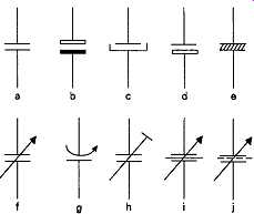
FIG. 5
With capacitors, as with most other circuit components, the capacitance value, together with the working voltage and the required precision of value, where these are important or non-standard, will be appended as a label, such as 2u2F/64V/10%. (It’s becoming normal practice for the magnifier symbol, such as 'p' or 'µ' or 'k' or 'M' to be used instead of the decimal point, as in the previous example.) Electrolytic capacitors, that is to say capacitors in which a thin insulating layer of metallic oxide has been formed within the component by electrolytic action, and which must therefore be connected in the circuit so that the applied voltage across its terminals has the correct polarity, are shown in the several forms illustrated in FIGs. 5b, 5c, or 5d, the actual symbol used depending on design office or national preferences.
Regrettably, the diagram of FIG. 5c is also some times used to denote a non-polar capacitor, as an alternative to that of FIG. 5a. This source of ambiguity could be avoided if a V polarity sign is always appended to the positive terminal of an electrolytic component. In some drawings of Japanese origin, electrolytic capacitors are depicted by the symbol shown in FIG. 5e.
Capacitors in which the value can be manually adjusted, known as 'variable capacitors', are shown in the forms illustrated in FIGs. 5f- 5k. A convention which is worth remembering, because it’s used with many other component symbols, is that an arrow with a point on its end usually implies that the component is intended to be adjusted frequently, for some operational or control purpose, whereas an arrow with a square end implies a pre-set component, which might be adjusted once, on setting up the equipment, and thereafter left alone.
FIGs. 5g and 5h frequently imply small value 'trimmer' capacitors, whereas FIG. 5f would be used most commonly to represent a larger value variable capacitor, used as the 'tuning' control in a radio receiver. A special form of tuning capacitor, used in transmitters and short-wave receivers, is the 'split stator' type, in which two insulated plates are separated by a central earthed plate. This is denoted by the diagram of FIG. 5j.
Where several variable capacitors are 'ganged' together, so that several sections can be adjusted simultaneously from the same control spindle, this fact is usually represented by the use of a dotted line joining the rear ends of the arrows together. The same dotted line convention is used to denote ganged sections of potentiometers and switches.
A similar diagram to that of FIG. 5j, shown in FIG. 5k, is used to denote a variable capacitor in which a sheet of some thin insulating material has been inserted between the plates so that these can be operated at much closer spacings, which allows a more compact component to be made, without the likelihood of an inadvertent short circuit occurring between the plates.
Resistors and potentiometers
The normal symbol for a fixed resistor is that shown in FIGs. 6a or 1.6b. The latter is becoming more popular because it’s easier to draw neatly, but is slightly more ambiguous in its appearance. A two terminal continuously variable resistor is represented by either of the FIGs. 6c or 1.6d, while a preset variable resistor is illustrated in FIGs. 6e or 1.6f . The label applied to a resistor will specify its ohmic value, and may also denote its type, for example wire wound (ww), metal film (mf) or metal oxide film (mo) as well as its power rating and precision in value, giving a description such as 2k2/3W/5%/ww.
A three-terminal potential divider (potentiometer) is shown by either FIG. 6g or 1.6h, depending on whether it’s of a continuously variable or preset form.
Note again the 'arrow head' convention. Using the oblong box type of resistor diagram, a continuously variable potentiometer would be shown as in FIG. 6k.
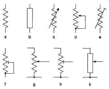
FIG. 6
Coils and transformers
The simplest form, that of a fixed value air cored coil, is illustrated in FIG. 7a. For RF use, in order to make the component more compact, a powdered iron core may be used, which will give the coil a higher inductance value for the same number of turns of winding. This is indicated by the use of the dotted line core shown in FIG. 7b. FIGs. 7c and 7d denote dust iron cored, or similar, coils in which the inductance can be adjusted by a preset or continuously variable position for the core.
The use of a laminated sheet iron core, for a low frequency choke, is indicated by FIG. 7e.
Radio frequency transformers are illustrated in FIGs. 7f , 7g and 7h, using air cores, and fixed and variable dust iron cores respectively. The diagram used in FIG. 7j is sometimes used to denote a variable dust iron core position, as an alternative to that of FIG. 7h. Where the coil or RF transformer is enclosed in a screening can, a box is drawn around it, as in FIG. 7k.
Where coils are inductively coupled, though not shown close to each other, this is indicated by a curving line drawn through both, as shown in FIG. 7m, and where the extent of such coupling is adjustable, this would be indicated by the arrow head symbol of FIG. 7n.
Low frequency power transformers, such as those used for mains power inputs, are depicted by the drawings of FIGs. 7p, 7q and 7r, of which the last two represent tapped and separated winding types.
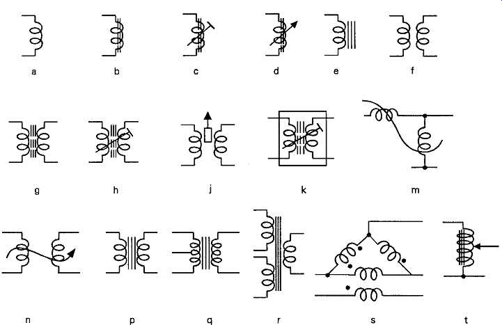
FIG. 7
If the direction of winding in a coil or transformer is important, the 'top' ends of all windings made in the same direction will be marked by a 'dot', as in FIG. 7s. By analogy with the symbol for a potentiometer, a 'Variac', or variable transformer, would be drawn as in FIG. 7t .
Switches
These are mainly drawn in a manner which closely follows their mechanical function, as for example the two-way switch of FIG. 8a and the five-way rotary switch shown in FIG. 8b. It’s conventional to indicate the moving arm by an arrow head symbol. In normally closed, and normally open forms, this may be indicated by an offset arrow head, as in FIGs. 8c and 8d.
Switches with ganged segments, such as the main power on/off switch for a piece of equipment, are commonly denoted by a dotted line linking the moving arms, as in FIG. 8e.
A momentary contact switch of the kind which makes contact only when the actuating button is de pressed is shown as in FIG. 8f . One in which the operation of the switch momentarily breaks the circuit would be drawn as in FIG. 8g.