AMAZON multi-meters discounts AMAZON oscilloscope discounts
Common DC Generator Characteristics
DC generators are used primarily for operation with mobile equipment. In industrial plants and commercial buildings, they are used for standby power, for battery charging, and for specialized DC operations such as electroplating. In many situations, rectification systems that convert AC to DC have replaced DC generators, since they are cheaper to operate and maintain.
DC generators supply power to a load circuit by converting the mechanical energy of some prime mover, such as a gasoline or diesel engine, into electrical energy. The prime mover must rotate at a definite speed in order to produce the desired voltage.
When DC generators operate, a characteristic known as armature re action takes place. The current through the armature windings produces a magnetic flux that reacts with the main field flux, as shown in FIG. 19.
The result is that a force is created that tends to rotate the armature in the opposite direction. As load current increases, the increase in armature cur rent causes a greater amount of armature reaction to take place. This condition can cause a considerable amount of sparking between the brushes and the commutator. However, armature reaction may be reduced by placing windings called interpoles between the main field windings of the stator. These windings are connected in series with the armature windings. Thus, an increase in armature current creates a stronger magnetic field around the interpoles, which counteracts the main field distortion created by the armature conductors.
Rating of DC Generator--The output of a DC generator is usually rated in kilowatts, which is the electrical power capacity of a machine. Other ratings, which are specified by the manufacturer on the nameplate of the machine, are current capacity, output voltage, speed, and temperature.
DC generators are made in a wide range of physical sizes, and with various electrical characteristics.
DC Generator Applications--DC generator use has declined rapidly since the development of the low-cost silicon rectifier. However, there are still certain applications where DC generators are used. These applications include railroad power systems, synchronous motor-generator units, power systems for large earth-moving equipment, and DC motor-drive units for precise equipment control.
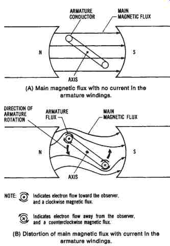
FIG. 19. Illustration of armature reaction: (A) Main magnetic flux with
no current flow in the armature windings, (B) Distortion of main magnetic
flux with cur rent flow in the armature windings
DC CONVERSION SYSTEMS
Most of the electrical power produced is 60-Hz three-phase alternating current. However, the use of direct current is necessary for many applications. For instance, DC motors have more desirable speed control and torque characteristics than AC motors. We have already discussed two methods of supplying direct current-batteries and DC generators. The fact that batteries and DC generators have been used as DC power sources for many years has been discussed. In many cases today, where large amounts of DC power are required, it is more economical to use a system for converting AC to DC. DC load devices may be powered by systems, called either rectifiers or converters, that change AC into a suitable form of DC.
Single-phase Rectification Systems
The simplest system for converting AC to DC is single-phase rectification. A single-phase rectifier changes AC to pulsating DC. The most common and economical method is the use of low-cost, silicon, semiconductor rectifiers.
Single-phase Half-wave Rectification
A single-phase half-wave rectifier circuit, such as shown in FIG. 20, converts an AC source voltage into a pulsating direct current. Let us assume that during the positive alternation of the AC cycle, the anode of the diode is positive ( FIG. 20). The diode will then conduct, since it is forward biased and the pn junction is low-resistant. The positive half cycle of the alternating current will then appear across the load device (represented by a resistor). When the negative portion of the AC alternation is input to the circuit, the anode of the diode becomes negative. The diode is now reverse biased, and no significant current will flow through the load device ( FIG. 20B). Therefore, there will be no voltage across the load.
The input and resulting output waveforms of the half-wave rectifier circuit are shown in FIG. 20C. The pulsating direct current of the output has an average DC level. The average value of the pulsating DC produced by single-phase half-wave rectification is expressed as:
Vd = 0.318 × Vmax
where:
Vdc = the average value of rectified voltage, and
Vmax = the peak (maximum) value of applied AC voltage.
Sample Problem:
Given: a single-phase, half-wave rectifier has 15 volts (rms) applied to its input.
Find: DC output voltage of the rectifier.
Solution:
Vdc = 0.318 × Vmax
= 0.318 × (15 V × 1.41)
Vdc = 6.72 volts
Certain diode ratings should be considered for half-wave rectifier circuits. The maximum forward current (Imax) is the largest current that can flow through the diode while it is forward biased, without damaging the device. The peak inverse voltage (piv) is the maximum voltage across the diode while it is reverse biased. For the half-wave rectifier, the maximum voltage developed across the diode is Vmax of the applied AC. As shown in the preceding formula, the piv of a diode used in a half-wave circuit must be much larger than the DC voltage developed.
Single-phase Full-wave Rectification
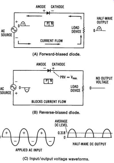
FIG. 20. Single-phase half-wave rectification: (A) Forward-biased diode,
(B) Reverse-biased diode, (C) Input/output voltage waveforms
In order to obtain a more pure form of DC energy, it is possible to improve upon half-wave rectification systems. FIG. 21 shows a single phase full-wave rectifier that uses two diodes and produces a DC output voltage during each alternation of the AC input. The rectified output of the full-wave rectifier has twice the DC voltage level of the half-wave rectifier.
The full-wave rectifier utilizes a center-tapped transformer to transfer AC source voltage to the diode rectifier circuit. During the positive half cycle of AC source voltage, the instantaneous charges on the transformer secondary are as shown in FIG. 21. The peak voltage (Vmax) is developed across each half of the transformer secondary. At this time, diode D1 is forward biased, and diode D2 is reverse biased. Therefore, conduction occurs from the center-tap, through the load device, through D1, and back to the outer terminal of the transformer secondary. The positive half cycle is developed across the load, as shown.
During the negative half cycle of the AC source voltage, diode D1 is re verse biased, and diode D2 is forward biased by the instantaneous charges shown in FIG. 21. The current path is from the center-tap, through the load device, through O2, and back to the outer terminal of the transformer secondary. The negative half cycle is also produced across the load, developing a full-wave output, as illustrated in FIG. 21.
Each diode in a full-wave rectifier circuit must have a piv rating of twice the value of the peak voltage developed at the output, since twice the peak voltage (2Vmax) is present across the diode when it is reverse biased. The average voltage for a full-wave rectifier circuit is:
Vdc = 2 (0.318 × Vmax)
= 0.636 × Vmax
Sample Problem:
Given: a single-phase, half-wave rectifier has 120 volts (rms) applied to its input.
Find: DC output voltage of the rectifier.
Solution:
Vdc = 0.636 × Vmax
= 0.636 × (120 V × 1.41)
Vdc = 107.61 volts
This type of rectifier circuit produces twice the DC voltage output of a half-wave rectifier circuit. However, it requires a bulky center-tapped transformer, as well as diodes that have a piv rating of twice the peak value of applied AC voltage.
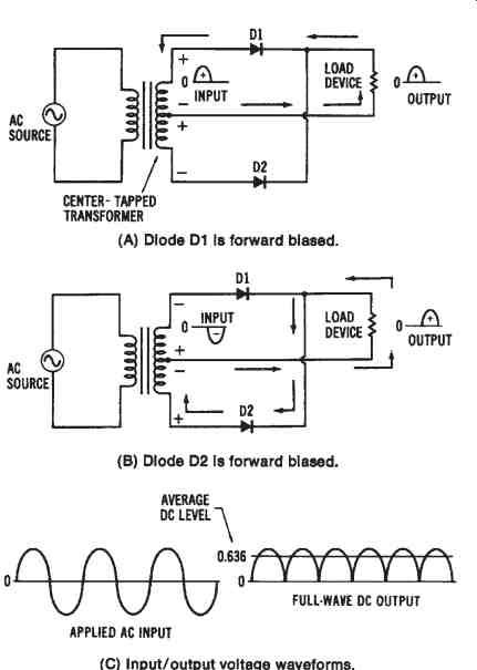
FIG. 21. Single-phase full-wave rectification: (A) Diode D1 is forward
biased, (B) Diode D2 is forward biased, (C) Input/output voltage waveforms
Single-phase Bridge Rectification
One disadvantage of the full-wave rectifier discussed previously is the requirement for a large center-tapped transformer. To overcome this disadvantage, four diodes may be used to form a full-wave bridge rectifier, as shown in FIG. 22. Additionally, the diode piv rating is only required to be the peak output voltage value (Vmax).
During the operation of a bridge rectifier, two diodes are forward biased during each alternation of the AC input. When the positive half cycle occurs, as shown in FIG. 22A, diodes D1 and D3 are forward biased, while diodes D2 and D4 are reverse biased. This biasing condition is due to the instantaneous charges occurring during the positive alternation. The conduction path is from the instantaneous negative side of the AC source, through diode D3, through the load device, through diode D1, and back to the instantaneous positive side of the AC source.
During the negative alternation of the AC input, diodes D2 and D4 are forward biased, while diodes 01 and 03 are reverse biased. Conduction occurs, as shown in FIG. 22B, from the instantaneous negative side of the source, through diode D2, through the load device, through diode 04, and back to the instantaneous positive side of the AC source. Since a voltage is developed across the load device during both half-cycles of the AC input, a full-wave output is produced, as shown in FIG. 22, that is similar to that of the full-wave rectifier discussed previously. For high values of DC output voltage, the use of a bridge rectifier is desirable, since the diode piv rating is one-half that of other single-phase rectification methods. A typical design of a bridge rectifier unit is shown in FIG. 22.
Three-phase Half-wave Rectification
Most industries are supplied with three-phase AC. It is therefore beneficial, because of the inherent advantages of three-phase power, to use three-phase rectifiers to supply DC voltage for industrial use. Single phase rectifiers are ordinarily used where low amounts of DC power are required. To supply larger amounts of DC power for industrial requirements, a three-phase rectifier circuit, such as the one shown in Figure 7 23, could be employed. Three-phase rectifier circuits produce a purer DC voltage output than single-phase rectifier circuits, thus wasting less AC power.
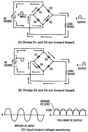
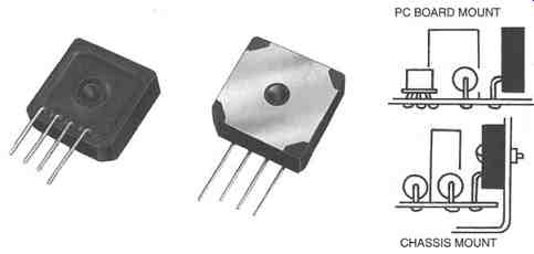
FIG. 22. Single-phase full-wave bridge rectification: (A) Diodes D1 an
D3 and forward biased, (B) Diodes D2 and D4 ore forward biased, (C) Input/output
voltage waveforms, (D) Printed circuit board rectifier unit (Electronic
Devices, Inc.)
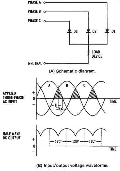 FIG. 23. Three-phase half-wave rectification: (A) Schematic diagram, (B)
Input/output voltage waveforms
FIG. 23. Three-phase half-wave rectification: (A) Schematic diagram, (B)
Input/output voltage waveforms
FIG. 23 shows a three-phase half-wave rectifier circuit that does not use a transformer. Phases A, B, and C of the wye-connected three-phase source supply voltage to the anodes of diodes D1, D2, and D3. The load device is connected between the cathodes of the diodes and the neutral point of the wye-connected source. Maximum conduction occurs through diode D1, since it is forward biased, when phase A is at its peak positive value. No conduction occurs through diode D1 during the negative alter nation of phase A. The other diodes operate in a similar manner, conducting during the positive AC input alternation and not conducting during the associated negative AC alternation. In a sense, this circuit combines three single-phase, half-wave rectifiers to produce a half-wave DC out-put, as shown in FIG. 23B. Of course, the voltages appearing across the diodes are 120° out of phase. There is a period of time during each AC cycle when the positive alternations overlap one another, as shown in the shaded areas of the diagram ( FIG. 23B). During the overlap time period t1, the phase A voltage is more positive than the phase B voltage, while during the t2, interval, the phase B voltage is more positive. Diode D1 will conduct until the time period t1 ends, then diode D2 will conduct, beginning at the end of t1 until the next area of overlapping is reached.
Note that voltage across the load device rises to a peak value twice during each phase alternation of the AC input voltage. These peaks are 120° apart. Since the DC output voltage never falls to zero, less AC ripple is present, which results in a purer form of DC than single-phase rectifiers produce. The average DC output voltage (Vdc) is expressed as:
Vdc = 0.831 × Vmax which compares very favorably with single-phase full-wave rectifier circuits.
Sample Problem:
Given: a three-phase, half-wave rectifier circuit has 240 volts (rms) applied to its input.
Find: the DC output voltage of the rectifier.
Solution:
Vdc = 0.831 × Vmax
= 0.831 × (240 V × 1.41)
Vdc = 281.2 volts
A disadvantage of this type of three-phase rectifier is that the AC lines are not isolated. Isolation is a direct connection to the AC lines; the lack of isolation could be a safety hazard. To overcome this disadvantage, a transformer may be used, as shown in FIG. 24, to form a similar three-phase, half-wave rectifier. The secondary voltage may be either in creased or decreased by the proper selection of the transformer, thus pro viding a variable DC voltage capability. The circuit illustrated in FIG. 24 has a delta-to-wye-connected transformer. The operation of this circuit is identical to that of the three-phase, half-wave rectifier previously discussed; however, line isolation has been accomplished.
Three-phase Full-wave Rectification
The full-wave counterpart of the three-phase, half-wave rectifier circuit is shown in FIG. 24A. This type of rectifier circuit is popular for many industrial applications. Six rectifiers are required for operation of the circuit. The anodes of D4, D5, and D6 are connected together at point A, while the cathodes of D1, D2, and D3 are connected together at point B. The load device is connected across these two points. The three-phase AC lines are connected to the anode-cathode junctions of D1 and D4, D2 and D5, and D3 and D6. This circuit does not require the neutral line of the three-phase source; therefore, a delta-connected source could be used.
The resulting DC output voltage of the three-phase, full-wave rectifier circuit is shown in FIG. 25B. The operation of the circuit is similar to that of a single-phase bridge rectifier in many respects. At any single instant of time during the three-phase AC input cycle, the anode voltage of one of the diodes is more positive than that of all the others, while the cathode voltage of another diode is more negative than that of all the others. These two diodes will then form the conduction path for that time period. This conducting action is similar to a bridge rectifier, since two di odes conduct during a time interval. Each rectifier in this circuit conducts during one-third of an AC cycle (120°). Peak positive DC output voltage occurs during every 60° of the three-phase AC input.
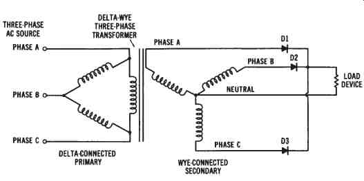
FIG. 24. Three-phase half-wave rectification using a transformer
Rotary Converters
Another method that has been used to convert AC to DC is the use of a rotary converter. Rotating AC-to-DC converters are seldom used today.
However, a motor-driven generator unit, such as shown in FIG. 26 can be used to convert DC to AC. This system is called an inverter. When operated as a converter to produce DC, the machine is run off an AC line.
The AC is transferred to the machine windings through slip rings and converted to DC by a split-ring commutator located on the same shaft. The amount of DC voltage output is determined by the magnitude of the AC voltage applied to the machine. Converters may be designed as two units, with motor and generator shafts coupled together, or as one unit housing both the motor and generator.
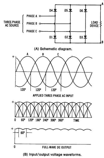
FIG. 25. Three-phase full-wave rectification: (A) Schematic diagram, (B)
Input/output voltage waveforms
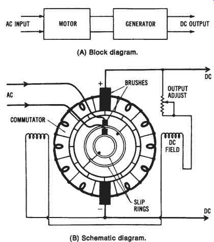
FIG. 26. Rotary AC-to-DC converter
DC FILTERING METHODS
The pulsating direct current produced by both single-phase and three phase rectifier circuits is not pure DC. A certain amount of AC ripple is evident in each type of rectifier. For many applications, a smooth DC output voltage, with the AC ripple removed, is required. Circuits used to remove AC variations of rectified DC are called filter circuits.
The output of a rectifier has a DC value and an AC ripple value, as shown in FIG. 27. To gain a relative index of the amount of AC variation, the ripple factor of a rectifier output waveform may be determined.
Ripple factor is expressed as:
Vr(rms)
r = --- Vdc where:
r = the ripple factor,
Vr(rms)
= the rms value of the AC component, and
Vdc = the average value of the rectified DC voltage.
Another index used to express the amount of AC ripple is the percent of ripple of a rectified DC voltage. Ripple percentage is expressed as:
Vr(rms)
% ripple = --- = 100
Vdc
Sample Problem:
Given: a power supply has an AC input of 24 volts (rms) and a p-p ripple of 1.5 volts at its output, as measured with an oscilloscope.
Find: DC voltage output of the power supply.
Solution:
Vr(p-p)
VDC = Vmax - --- 2
1.5 V
= (24 V × 1.41) - --- 2
VDC = 33.09 volts
A full-wave rectified voltage has a lower percentage of ripple than a half-wave rectified voltage. When a DC supply must have a low amount of ripple, a full-wave rectifier circuit should be used.
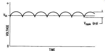 FIG. 27. Rectifier output voltage
Capacitor Filter
A simple capacitor filter may be used to smooth the AC ripple of a rectifier output. FIG. 28 shows the result of adding a capacitor across the output of a single-phase, full-wave bridge rectifier. The output waveform after the capacitor has been added is shown in FIG. 28C.
The ideal filtered DC voltage would be one with no AC ripple and a value equal to the peak voltage (Vmax) from the rectifier output. Note that in FIG. 28, the value of Vdc is approaching that of Vmax, and compare this to the full-wave rectified voltage of FIG. 28. There are two time intervals shown in FIG. 28. Time period t1 represents diode conduction that charges the filter capacitor (C) to the peak rectified voltage (Vmax). Time period t2 is the time required for the capacitor to discharge through the load (RL).
If a different value of filter capacitor were put into the circuit, a change in the rate of discharge would result. If capacitor C discharged a very small amount, the value of Vdc would be closer to the value of Vmax.
With light loads (high resistance), the capacitor filter will supply a high DC voltage with little ripple. However, with a heavy (low resistance) load connected, the DC voltage would drop, because of a greater ripple. The in creased ripple is caused by the lower resistance discharge path for the filter capacitor. The effect of an increased load on the filter capacitor is shown in FIG. 28.
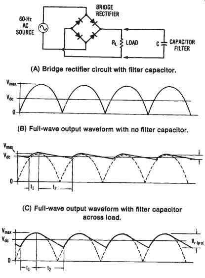
FIG. 28. Filter capacitor operation: (A) Bridge rectifier circuit with
filter capacitor, (8) Full-wave output waveform with no filter capacitor,
(C) Full-wove output waveform with filter capacitor across load, (D) Full-wave
output wave form with filter capacitor across heavier (lower resistance)
load
By utilizing the value indicated on the waveforms of FIG. 28, it is possible to express Vdc and Vr(rms) as:
Vr(p-p)
Vdc = Vmax - --- 2 and
Vr(p-p)
Vr(rms)
= --- 2 × v3
Sample Problem:
Given: the measured AC ripple voltage at the output of a filtered power supply is 0.8V (rms), and the DC output voltage is 15.0 volts.
Find: the percent ripple of the power supply.
Solution:
0.8V × 100
%r = ----- 15.0 V
= 5.33%
Sample Problem:
Given: a power supply has a p-p ripple of 1.2 volts at its output.
Find: the rms ripple voltage of the power supply.
It should be pointed out that as the value of C increases, the value of the peak current through the diodes will also increase. There is, therefore, a practical limit for determining the value of C that is reflected in the fore going equation.
The capacitor filter produces a high DC voltage with low AC ripple for light loads. However, its major disadvantages are higher ripple and lower Vdc at heavier loads, poor voltage regulation, and high peak cur rent through the diodes.
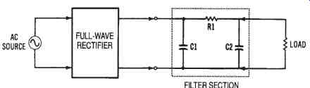
FIG. 29. An RC filter circuit
RC Filter
It is possible to improve upon the previous filter circuit by using an RC filter. FIG. 29 shows an RC filter stage. This filter has lower ripple than a capacitor filter, but has a lower average DC voltage, because the voltage is dropped across R1.
The purpose of R1 and C2 is to add another filter network, in addition to C1, to further reduce the ripple. This circuit also operates best with light loads connected. It is possible to have many stages of RC filters to further reduce AC ripple.
Pi- or p-type Filter
The use of the resistor (R1) in the RC filter is not desirable in many cases, since it reduces the average DC output of the circuit. To compensate for the DC voltage reduction, a pi-type (or p-type) filter may be used. FIG. 30 shows this type of filter. The advantage of the choke coil (L1) over the resistor (R1) of the RC filter is that it offers only a small DC series resistance, but its AC impedance is much larger. It therefore passes DC and blocks the AC component of the rectified voltage.
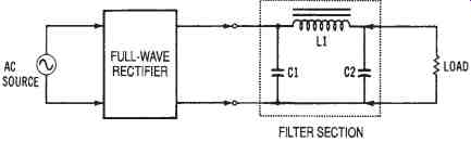
FIG. 30. A pi-type filter circuit
DC REGULATION METHODS
The concept of voltage regulation can best be understood by referring to the formula:
VNL - VFL × 100
VR = ------- VFL where:
VR = the voltage regulation in percent,
VNL = the no-load (open-circuit) voltage, and
VFL the rated, full-load voltage.
In an ideally regulated circuit, VNL would equal VFL.
In all types of power supplies that convert AC to DC, the DC output levels are affected by variations in the load. The lower the percentage of regulation (approaching 0 percent), the better regulated the circuit is. For instance, power supplies are capable of having a voltage regulation of less than 0.01 percent, which means that the value of the load has little effect on the DC output voltage produced. A well-regulated DC power supply is necessary for many industrial applications.
Voltage Regulators
A simple voltage regulation circuit that uses a zener diode is shown in FIG. 31. This circuit consists of a series resistor (Rs) and a zener diode (D1) connected to the output of a rectifier circuit. However, we should re view zener diode operation before discussing the circuit operation.
Zener diodes are similar to conventional diodes when they are forward biased. When they are reverse biased, no conduction takes place until a specific value of reverse breakdown voltage (or "zener" voltage) is reached. The zener is designed so that it will operate in the reverse breakdown region of its characteristic curve (see FIG. 31B). The reverse breakdown voltage is predetermined by the manufacturer. When used as a voltage regulator, the zener diode is reverse biased so that it will operate in the breakdown region. In this region, changes in current through the diode have little effect on the voltage across it. The constant-voltage characteristic of a zener diode makes it desirable for use as a regulating device.
The circuit of FIG. 31A is a zener diode shunt regulator. The zener establishes a constant voltage across the load resistance within a range of rectified DC voltages and output load currents. Over this range, the volt age drop across the zener remains constant. The current through the zener (IZ) will vary to compensate for changes in load resistance, since IZ = IT - IL. Thus, the output voltage will remain constant.
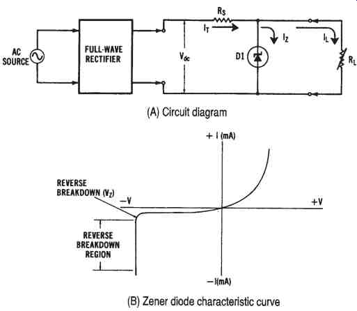
FIG. 31. Zener diode voltage regulator: (A) Circuit diagram, (B) Zener
diode characteristic curve
Transistor Voltage Regulators
An improvement over the zener voltage regulator is a transistorized regulator, as shown in the circuit in FIG. 32. This regulator has transistor Q1 placed in series with the load device (RL). Transistor Q1, then, acts to produce variable resistance to compensate for changes in the input voltage. The collector-emitter resistance of Q1 varies automatically with changes in the circuit conditions. The zener diode establishes the DC bias placed on the base of transistor Q1. When this circuit is operating properly, if the voltage across the load increases, the rise in emitter voltage makes the base less positive. The current through Q1 will then be reduced, which results in an increase in the collector-emitter resistance of Q1. The increase in resistance will cause a larger voltage drop across transistor Q1, which will now compensate for the change in voltage across the load. Opposite conditions would occur if the load voltage were to decrease. Many variations of this circuit are used in regulated power supplies today.
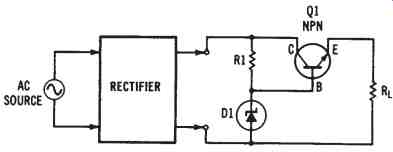
FIG. 32. Transistor series voltage regulator circuit
FIG. 33. Transistor shunt voltage regulator circuit
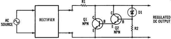
Shunt regulators are also used in DC power supplies. The circuit of FIG.
33 is a shunt voltage regulator. Again, the zener diode (D1) is used
to establish a constant DC bias level. Therefore, voltage variations across
the DC output will be sensed only by resistor R2. If the DC output voltage
rises, an increased positive voltage will be present at the base of transistor
Q2. The increased forward bias on transistor Q2 will cause it to conduct
more. This makes the base of transistor Q1 more positive, and Q1 will
then conduct more heavily. Increased current flow through both transistors
causes an increase in the voltage drop across resistor R1. This increased voltage
drop across R1 will counterbalance the rise in output voltage. Thus,
the DC output voltage will remain stabilized. Decreases in DC output voltage
would cause the circuit action to reverse. In addition, integrated circuit
voltage regulators are now used extensively in power supplies that convert
AC to DC.
