AMAZON multi-meters discounts AMAZON oscilloscope discounts
1. Introduction
2. Market Drivers
3. Optical Absorption: Introduction • Semiconductor Materials • Generation of EHP by Photon Absorption
4. Extrinsic Semiconductors and the pn Junction: Extrinsic Semiconductors • pn Junction
5. Maximizing Cell Performance: Externally Biased pn Junction • Parameter Optimization • Minimizing Cell Resistance Losses
6. Traditional PV Cells: Introduction • Crystalline Silicon Cells • Amorphous Silicon Cells • Copper Indium Gallium Diselenide Cells • Cadmium Telluride Cells • Gallium Arsenide Cells
7. Emerging Technologies: New Developments in Silicon Technology • CIS-Family-Based Absorbers • Other III-V and II-VI Emerging Technologies • Other Technologies
8. PV Electronics and Systems: Introduction • PV System Electronic Components
9. Conclusions
1. Introduction
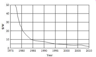
Above: Fig. 1 The decline in cost per watt for photovoltaic modules. (Data
from Maycock, P.D., Ed., Photovoltaic News, 18(1), 1999; From International
Marketing Data and Statistics, 22nd edn., Euromonitor PIC, London, U.K., 1998;
From Maycock, P.D., Renewable Energy World, 5, 147, 2002; From Earth Policy
Institute, Eco-Economy Indicators: Solar Power-Data www.earth-policy.org/Indicators/Solar/2007_data.htm.)
Becquerel first discovered that sunlight can be converted directly into electricity in 1839, when he observed the photo-galvanic effect. After more than a century of theoretical work, the first solar cell was not developed until 1954, by Chapin, Fuller, and Pearson, when sufficiently pure semiconductor material had become available. It had an efficiency of 6%. Only 4 years later, the first solar cells were used on the Vanguard I orbiting satellite.
As is often the case, extraterrestrial use of a technology has led to the terrestrial use of the technology. For extraterrestrial cells, the power:weight ratio was the determining factor for their selection, since weight was the expensive part of the liftoff equation. Reliability, of course, was also of paramount importance. Hence, for extraterrestrial power generation, the cost of the photovoltaic (PV) cells was secondary, provided that they met the primary objectives.
A new objective for PV cells emerged following the organization of the petroleum exporting countries (OPEC) petroleum embargo of the early 1970s, which highlighted the need to seek out alternative energy sources. In addition, the observation that fossil fuel sources pollute the atmosphere, water and soil with a number of pollutants such as SOx, NOx, particulates, and CO2 suggested that alternative sources should involve minimal air or water pollution. And, of course, perhaps the most desirable aspect of any new source would be an unlimited supply of fuel, as opposed to the observed dwindling supplies of domestic petroleum.
Solar energy became the obvious choice for alternative energy, either in the form of electricity via the PV effect or via solar thermal heating of water or other substances. But it would be necessary to significantly reduce the cost of capturing the solar resource before it could be used as a replacement for the relatively inexpensive fossil sources.
Since the events of the mid-1970s, the cost per watt of PV cells has declined steadily. Fig.1 shows an average decline of approximately 7%/year between 1980 and 2010, which represents a 50% drop every 10 years. In fact, between 2005 and 2010, the price dropped by 50% in a 5 year period.
Installations have grown from tens of kilowatts to thousands of megawatts per year, and continue to grow at a rapid rate. Recent rapid growth and accompanying declines in prices can be accounted for by a number of aggressive incentive programs around the world, such as in Germany, Spain, China, and California. For example, Germany now produces more than 20% of its electrical energy by renewable sources. Costa Rica will soon produce nearly 100% of its electrical energy needs from renewable sources, but in this case, hydroelectric and wind will be the major contributors to the renewable portfolio.
2. Market Drivers
Price, efficiency, performance, warranties, incentives, interest rates, money availability, space availability, and sometimes aesthetics have been the primary market drivers for current PV technologies. In fact, the decision to install generally involves consideration of all these factors.
Certainly price is important, but obviously if an inexpensive module will cost half as much as another module, but will last only 25% as long, the more expensive module will have a more attractive lifecycle cost. In many instances, where space is limited, the system owner will want to install as much power as possible in the available space in order to generate as much energy as possible. Where space is a consideration, then the metric for PV system selection is based upon kWh/m^2/year/$ for the energy produced by the system. And, in fact, generally the monetary consideration is only secondary to the energy production consideration.
Probably the most important driver among the remaining factors is incentive programs. It has been clearly demonstrated in Germany, Spain, California, New Jersey, Ontario, and a number of other countries, states, and cities that an attractive incentive program will encourage people to install PV systems on their homes and businesses. Incentive programs may take the form of one time rebates or tax credits or they may take the form of a guaranteed premium price paid over a guaranteed time period for the energy produced by the renewable system. In the final analysis, the owner of a system has a greater incentive as the payback time of the system decreases. Generally, if a system will pay for itself with the value of the energy it produces within a 6 year period, it’s a very attractive investment for a homeowner and an acceptable investment for many businesses.
The trade-off must be the impact on utility ratepayers, since, generally the funding for the incentive comes either directly from the utility or indirectly via government loans or grants, which, ultimately, are paid for by the taxpayer, who is most likely a ratepayer. Incentive programs must be carefully crafted to ensure acceptance by those who wish to install systems, but not to impose an excessive cost burden on the general population. Just as the energy produced must be sustainable, the incentive program must also be sustainable.
3. Optical Absorption
3.1 Introduction
When light shines on a material, it’s reflected, transmitted, or absorbed. Absorption of light is simply the conversion of the energy contained in the incident photon to some other form of energy, typically heat. Some materials, however, happen to have just the right properties needed to convert the energy in the incident photons to electrical energy.
3.2 Semiconductor Materials
Semiconductor materials are characterized as being perfect insulators at absolute zero temperature, with charge carriers being made available for conduction as the temperature of the material is increased.
This phenomenon can be explained on the basis of quantum theory, by noting that semiconductor materials have an energy band gap between the valence band and the conduction band. The valence band represents the allowable energies of valence electrons that are bound to host atoms. The conduction band represents the allowable energies of electrons that have received energy from some mechanism and are now no longer bound to specific host atoms.
As temperature of a semiconductor sample is increased, sufficient energy is imparted to a small fraction of the electrons in the valence band for them to move to the conduction band. In effect, these electrons are leaving covalent bonds in the semiconductor host material. When an electron leaves the valence band, an opening is left which may now be occupied by another electron, provided that the other electron moves to the opening. If this happens, of course, the electron that moves in the valence band to the opening, leaves behind an opening in the location from which it moved. If one engages in an elegant quantum mechanical explanation of this phenomenon, it must be concluded that the electron moving in the valence band must have either a negative effective mass and a negative charge or, alternatively, a positive effective mass and a positive charge. The latter has been the popular description, and, as a result, the electron motion in the valence band is called hole motion, where "holes" is the name chosen for the positive charges, since they relate to the moving holes that the electrons have left in the valence band.
What is important to note about these conduction electrons and valence holes is that they have occurred in pairs. Hence, when an electron is moved from the valence band to the conduction band in a semiconductor by whatever means, it constitutes the creation of an electron-hole pair (EHP). Both charge carriers are then free to become a part of the conduction process in the material.
3.3 Generation of EHP by Photon Absorption
The energy in a photon is given by the familiar equation,
where:
h is Planck's constant (h = 6.63 × 10⁻³⁴
J s) c is the speed of light (c = 2.998 × 10^8 m/s)
? is the frequency of the photon in Hertz
? is the wavelength of the photon in meters Since energies at the atomic level are typically expressed in electron volts (1 eV = 1.6 × 10^-19 J) and wavelengths are typically expressed in micrometers, it’s possible to express hc in appropriate units, so that if ....
? is expressed in µm, then E will be expressed in eV. The conversion yields:
The energy in a photon must exceed the semiconductor bandgap energy, Eg, to be absorbed. Photons with energies at and just above Eg are most readily absorbed because they most closely match bandgap energy and momentum considerations. If a photon has energy greater than the bandgap, it still can pro duce only a single EHP. The remainder of the photon energy is lost to the cell as heat. It’s thus desirable that the semiconductor used for photoabsorption have a bandgap energy such that a maximum percent age of the solar spectrum will be efficiently absorbed.
Now, note that the solar spectrum peaks at ? ˜ 0.5 µm. Equation 1b shows that a bandgap energy of approximately 2.5 eV corresponds to the peak in the solar spectrum. In fact, since the peak of the solar spectrum is relatively broad, bandgap energies down to 1.0 eV can still be relatively efficient absorbers, and in certain special cell configurations, even smaller bandgap materials are appropriate.
The nature of the bandgap also affects the efficiency of absorption in a material. A more complete representation of semiconductor bandgaps must show the relationship between bandgap energy as well as bandgap momentum. As electrons make transitions between conduction band and valence band, both energy and momentum transfer normally take place, and both must be properly balanced in accordance with conservation of energy and conservation of momentum laws.
Some semiconducting materials are classified as direct bandgap materials, while others are classified as indirect bandgap materials. Fig.2 [6] shows the bandgap diagrams for two materials considering momentum as well as energy. Note that for silicon, the bottom of the conduction band is displaced in the momentum direction from the peak of the valence band. This is an indirect bandgap, while the GaAs diagram shows a direct bandgap, where the bottom of the conduction band is aligned with the top of the valence band.
What these diagrams show is that the allowed energies of a particle in the valence band or the conduction band depend on the particle momentum in these bands. An electron transition from a point in the valence band to a point in the conduction band must involve conservation of momentum as well as energy. For example, in Si, even though the separation of the bottom of the conduction band and the top of the valence band is 1.1 eV, it’s difficult for a 1.1 eV photon to excite a valence electron to the conduction band because the transition needs to be accompanied with sufficient momentum to cause displacement along the momentum axis, and photons carry little momentum. The valence electron must thus simultaneously gain momentum from another source as it absorbs energy from the incident photon. Since such simultaneous events are unlikely, absorption of photons at the Si bandgap energy is several orders of magnitude less likely than absorption of higher energy photons.
Since photons have so little momentum, it turns out that the direct bandgap materials, such as gallium arsenide (GaAs), cadmium telluride (CdTe), copper indium diselenide (CIS), and amorphous silicon (a-Si:H) absorb photons with energy near the material bandgap energy much more readily than do the indirect materials, such as crystalline silicon. As a result, the direct bandgap absorbing material can be several orders of magnitude thinner than indirect bandgap materials and still absorb a significant part of the incident radiation.
===
1.43 eV 1.1 eV Conduction band Conduction band Valence band Valence band Si GaAs
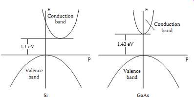
Above: Fig. 2 The energy and momentum diagram for valence and conduction
bands in Si and GaAs.
===
The absorption process is similar to many other physical processes, in that the change in intensity with position is proportional to the initial intensity. As an equation, this becomes displacement along the momentum axis, and photons carry little momentum. The valence electron must thus simultaneously gain momentum from another source as it absorbs energy from the incident photon. Since such simultaneous events are unlikely, absorption of photons at the Si bandgap energy is several orders of magnitude less likely than absorption of higher energy photons.
Since photons have so little momentum, it turns out that the direct bandgap materials, such as gallium arsenide (GaAs), cadmium telluride (CdTe), copper indium diselenide (CIS), and amorphous silicon (a-Si:H) absorb photons with energy near the material bandgap energy much more readily than do the indirect materials, such as crystalline silicon. As a result, the direct bandgap absorbing material can be several orders of magnitude thinner than indirect bandgap materials and still absorb a significant part of the incident radiation.
The absorption process is similar to many other physical processes, in that the change in intensity with position is proportional to the initial intensity. As an equation, this becomes
dI dx
= I, -a
with the solution
I = I e , o x -a
where
I is the intensity of the light at a depth x in the material Io is the intensity at the surface a is the absorption constant
The absorption constant depends on the material and on the wavelength. At energies above the band gap, the absorption constant increases relatively slowly for indirect bandgap semiconductors and increases relatively quickly for direct bandgap materials. Equation 3 shows that the thickness of material needed for significant absorption needs to be several times the reciprocal of the absorption constant.
This is important information for the designer of a PV cell, since the cell must be sufficiently thick to absorb the incident light.
In any case, when the photon is absorbed, it generates an EHP. The question, then, is what happens to the EHP?
4. Extrinsic Semiconductors and the pn Junction
4.1 Extrinsic Semiconductors
At T = 0 K, intrinsic semiconductors, i.e., semiconductor materials with no impurities, have all covalent bonds completed with no leftover electrons or holes. If certain impurities are introduced into intrinsic semiconductors, there can be leftover electrons or holes at T = 0 K. For example, consider silicon, which is a group IV element, which covalently bonds with four nearest neighbor atoms to complete the outer electron shells of all the atoms. At T = 0 K, all the covalently bonded electrons are in place, whereas at room temperature, about one in 10^12 of these covalent bonds will break, forming an EHP, resulting in minimal charge carriers for current flow.
If, however, phosphorous, a group V element, is introduced into the silicon in small quantities, such as one part in 10^6 , four of the valence electrons of the phosphorous atoms will covalently bond to the neighboring silicon atoms, while the fifth valence electron will have no electrons with which to covalently bond. This fifth electron remains weakly coupled to the phosphorous atom, readily dislodged by temperature, since it requires only 0.04 eV to excite the electron from the atom to the conduction band. At room temperature, sufficient thermal energy is available to dislodge essentially all of these extra electrons from the phosphorous impurities. These electrons thus enter the conduction band under thermal equilibrium conditions, and the concentration of electrons in the conduction band becomes nearly equal to the concentration of phosphorous atoms, since the impurity concentration is normally on the order of 10^8 times larger than the intrinsic carrier concentration.
Since the phosphorous atoms donate electrons to the material, they are called donor atoms and are represented by the concentration, ND. Note that the phosphorous, or other group V impurities, don’t add holes to the material. They only add electrons. They are thus designated as n-type impurities.
On the other hand, if group III atoms such as boron are added to the intrinsic silicon, they have only three valence electrons to covalently bond with nearest silicon neighbors. The missing covalent bond appears the same as a hole, which can be released to the material by applying a small amount of thermal energy. Again, at room temperature, nearly all of the available holes from the group III impurity are donated to the conduction process in the host material. Since the concentration of impurities will normally be much larger than the intrinsic carrier concentration, the concentration of holes in the material will be approximately equal to the concentration of p-type impurities.
Historically, group III impurities in silicon have been viewed as electron acceptors, which, in effect, donate holes to the material. Rather than being termed hole donors, however, they have been called acceptors. Thus, acceptor impurities donate holes, but no electrons, to the material and the resulting hole density is approximately equal to the density of acceptors, which is represented as NA.
An interesting property of free electrons and holes is that they like each other. In fact, when they are close to each other, they have a strong tendency to recombine. This observation can be expressed as…
… where no represents the thermal equilibrium concentration of free electrons at a point in the semiconductor crystal po represents the thermal equilibrium concentration of holes ni represents the concentration of intrinsic charge carriers T is the temperature in K K is a constant that depends upon the material Note that in intrinsic material, no ? po = ni
… since, by definition, the intrinsic material has no impurities that affect the electrical properties of the material.
In Si, For example, which has approximately 10^22 covalent bonds/cm^3 , approximately 1 in 10^12 bonds creates an EHP at room temperature. This means that at room temperature for Si, ni
? 10^10/cm^3
Equation 4 shows that adding a mere one part per million of a donor or acceptor impurity can increase the free charge carrier concentration of the material by a factor of 10^6 for silicon. Equation 4 also shows that in thermal equilibrium, if either an n-type or a p-type impurity is added to the host material, that the concentration of the other charge carrier will decrease dramatically, since it’s still necessary to satisfy under thermal equilibrium conditions.
In extrinsic semiconductors, the charge carrier with the highest concentration is called the majority carrier and the charge carrier with the lowest concentration is called the minority carrier. Hence, electrons are majority carriers in n-type material, and holes are minority carriers in n-type material. The opposite is true for p-type material.
If both n-type and p-type impurities are added to a material, then whichever impurity has the higher concentration, will become the dominant impurity. However, it’s then necessary to acknowledge a net impurity concentration that is given by the difference between the donor and acceptor concentrations.
If, For example, ND > NA, then the net impurity concentration is defined as Nd = ND - NA. Similarly, if NA > ND, then Na = NA - ND.
4.2 pn Junction
4.2.1 Junction Formation and Built-In Potential
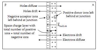
Above: Fig. 3 The pn junction showing electron and hole drift and diffusion.
Although n-type and p-type materials are interesting and useful, the real fun starts when a junction is formed between n-type and p-type materials. The pn junction is treated in gory detail in most semiconductor device theory textbooks. Here, the need is to establish the foundation for the establishment of an electric field across a pn junction and to note the effect of this electric field on photo-generated EHPs.
Fig.3 shows a pn junction formed by placing p-type impurities on one side and n-type impurities on the other side. There are many ways to accomplish this structure. The most common is the diffused junction.
When a junction is formed, the first thing to happen is that the conduction electrons on the n-side of the junction notice the scarcity of conduction electrons on the p-side, and the valence holes on the p-side notice the scarcity of valence holes on the n-side. Since both types of charge carrier are undergoing random thermal motion, they begin to diffuse to the opposite side of the junction in search of the wide open spaces. The result is diffusion of electrons and holes across the junction, as indicated in Fig.3.
When an electron leaves the n-side for the p-side, however, it leaves behind a positive donor ion on the n-side, right at the junction. Similarly, when a hole leaves the p-side for the n-side, it leaves a negative acceptor ion on the p-side. If large numbers of holes and electrons travel across the junction, large numbers of fixed positive and negative ions are left at the junction boundaries. These fixed ions, as a result of Gauss' law, create an electric field that originates on the positive ions and terminates on the negative ions.
Hence, the number of positive ions on the n-side of the junction must be equal to the number of negative ions on the p-side of the junction.
The electric field across the junction, of course, gives rise to a drift current in the direction of the electric field. This means that holes will travel in the direction of the electric field and electrons will travel opposite the direction of the field, as shown in Fig.3. Notice that for both the electrons and for the holes, the drift current component is opposite the diffusion current component. At this point, one can invoke Kirchhoff's current law to establish that the drift and diffusion components for each charge carrier must be equal and opposite, since there is no net current flow through the junction region. This phenomenon is known as the law of detailed balance.
By setting the sum of the electron diffusion current and the electron drift current equal to zero, it’s possible to solve for the potential difference across the junction in terms of the impurity concentrations on either side of the junction. Proceeding with this operation yields ...
At this point, a word about the region containing the donor ions and acceptor ions is in order. Note first that outside this region, electron and hole concentrations remain at their thermal equilibrium values.
Within the region, however, the concentration of electrons must change from the high value on the n-side to the low value on the p-side. Similarly, the hole concentration must change from the high value on the p-side to the low value on the n-side. Considering that the high values are really high, i.e., on the order of 10^18 /cm^3 , while the low values are really low, i.e., on the order of 10^2/cm^3 , This means that within a short distance of the beginning of the ionized region, the concentration must drop significantly below the equilibrium value. Because the concentrations of charge carriers in the ionized region are so low, this region is often termed the depletion region, in recognition of the depletion of mobile charge carriers in the region. Furthermore, because of the charge due to the ions in this region, the depletion region is also often referred to as the space charge layer. For the balance of this section, this region will simply be referred to as the junction.
The next step in the development of the behavior of the pn junction in the presence of sunlight is to let the sun shine in and see what happens.
Above: Fig. 4 The illuminated pn junction showing desirable geometry and the creation of electron-hole pairs.
Note: * At all EHP locations.
4.2.2 Illuminated pn Junction
Equation 3 governs the absorption of photons at or near a pn junction. Noting that an absorbed pho ton releases an EHP, it’s now possible to explore what happens after the generation of the EHP. Those EHPs generated within the pn junction will be considered first, followed by the EHPs generated outside, but near the junction, and then by EHPs generated further from the junction boundary.
If an EHP is generated within the junction, as shown in Fig.4 (points B and C), both charge carriers will be acted upon by the built-in electric field. Since the field is directed from the n-side of the junction to the p-side of the junction, the field will cause the electrons to be swept quickly toward the n-side and the holes to be swept quickly toward the p-side. Once out of the junction region, the optically generated carriers become a part of the majority carriers of the respective regions, with the result that excess concentrations of majority carriers appear at the edges of the junction. These excess majority carriers then diffuse away from the junction toward the external contacts, since the concentration of majority carriers has been enhanced only near the junction.
The addition of excess majority charge carriers to each side of the junction results in either a voltage between the external terminals of the material or a flow of current in the external circuit or both. If an external wire is connected between the n-side of the material and the p-side of the material, a current, I1, will flow in the wire from the p-side to the n-side. This current will be proportional to the number of EHPs generated in the junction region, which, in turn, will be proportional to the intensity of the incident light (irradiation).
If an EHP is generated outside the junction region, but close to the junction (with "close" yet to be defined, but shown as point A in Fig.4), it’s possible that, due to random thermal motion, either the electron, the hole, or both will end up moving into the junction region. Suppose that an EHP is generated in the n-region close to the junction. Then suppose that the hole, which is the minority carrier in the n-region, manages to reach the junction before it recombines. If it can do this, it will be swept across the junction to the p-side and the net effect will be the same as if the EHP had been generated within the junction, since the electron is already on the n-side as a majority carrier. Similarly, if an EHP is generated within the p-region, but close to the junction, and if the minority carrier electron reaches the junction before recombining, it will be swept across to the n-side where it’s a majority carrier. So what is meant by close? Clearly, the minority carriers of the optically generated EHPs outside the junction region must not recombine before they reach the junction. If they do, then, effectively, both carriers are lost from the conduction process, as in point D in Fig.4. Since the majority carrier is already on the correct side of the junction, the minority carrier must therefore reach the junction in less than a minority carrier lifetime, tn or tp.
To convert these times into distances, it’s necessary to note that the carriers travel by diffusion once they are created. Since only the thermal velocity has been associated with diffusion, but since the thermal velocity is random in direction, it’s necessary to introduce the concept of minority carrier dif fusion length, which represents the distance, on the average, which a minority carrier will travel before it recombines. The diffusion length can be shown to be related to the minority carrier lifetime and dif fusion constant by the formula:
L = D , m m m t
…where m has been introduced to represent n for electrons or p for holes. It can also be shown that on the average, if an EHP is generated within a minority carrier diffusion length of the junction, the associated minority carrier will reach the junction. In reality, some minority carriers generated closer than a diffusion length will recombine before reaching the junction, while some minority carriers generated farther than a diffusion length from the junction will reach the junction before recombining.
Hence, to maximize photocurrent, it’s desirable to maximize the number of photons that will be absorbed either within the junction or within a minority carrier diffusion length of the junction. The minority carriers of the EHPs generated outside this region have a higher probability of recombining before they have a chance to diffuse to the junction. If a minority carrier from an optically generated EHP recombines before it crosses the junction and becomes a majority carrier, it, along with the opposite carrier with which it recombines, is no longer available for conduction. The engineering design challenge then lies in maximizing a as well as maximizing the junction width and minority carrier dif fusion lengths. Additional information about the optimization of cell performance emerges when the performance of the cell under external bias is explored.
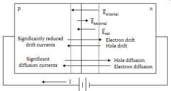
Above: Fig. 5 The pn junction with external bias.