AMAZON multi-meters discounts AMAZON oscilloscope discounts
<< cont. from part 1
4. Output Section
In general the output section of any switching power supply is comprised of single or multiple DC voltages, which are derived by direct rectification and filtering of the transformer secondary voltages and in some cases further filtering by series-pass regulators. These outputs are normally low-voltage, direct current, and capable of delivering a certain power level to drive electronic components and circuits. The most common output DC voltages are 5V, 12V, 15V, 24V, or 28V DC, and their power capability may vary from a few watts to thousands of watts.
The most common type of secondary voltages that have to be rectified in a switching power supply are high-frequency square waves. These in turn require special components, such as Schottky or fast recovery rectifiers, low ESR capacitors, and energy storage inductors, in order to produce low noise outputs useful to the majority of electronic components.
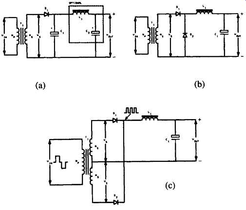
FGR. 10 Output stages (a) Flyback type (b) Forward type (c) Push-pull/half-
bridge/full-bridge
4.1 Output Rectification and Filtering Schemes
The output rectification and filtering scheme used in a power supply depends on the type of supply topology the designer chooses to use. The conventional fly back converter uses the output scheme shown in Fgr. 10(a). Since the transformer T l in the flyback converter also acts as an energy storing inductor, diode D 1, and capacitor C l are the only two elements necessary to produce a DC output.
Some practical designs, however, may require the optional insertion of an additional LC filter, shown in Fgr. 10(a) to suppress high-frequency switching spikes. The physical and electrical values of both L 1 and C 2 will be small. For the flyback converter, the rectifier diode D 1 must have a reverse voltage rating of:
[ 1.2Vin (Ns/Np)], minimum.
The output section of a forward converter is shown in Fgr. 10(b). Notice the distinct differences in the scheme compared to the flyback. Here, an extra diode D 2 called the flywheel, is added and also inductor L l precedes the smoothing capacitor. Diode D 2 provides current to the output during the off period. Therefore, the combination of diodes D l and D 2 must be capable of delivering full output current, while their reverse blocking voltage capabilities will be equal to [1.2Vin (Ns/Np)], minimum.
The output section that is shown in Fgr. 10(c) is used for push-pull, half bridge, and full-bridge converters. Since each of the two diodes D l and D 2 provides current to the output for approximately half of the cycle, they share the load current equally. An interesting point is that no flywheel diode is needed, because either diode acts as a flywheel when the other one is turned off. Either diode must have a reverse blocking capability of [2.4Vou t (Vin,max/Vin,min)], minimum.
4.2 Magnetic Amplifiers and Secondary Side Regulators
The magnetic-amplifier technology has been around for a long time, but renewed interest has emerged lately, especially with the proliferation of the switching regulator, as an efficient means of regulating the auxiliary outputs of a multiple output switching power supply. Mag amp output regulators have recently become very popular as a means of regulating more than one output of a switching power supply. They offer extremely precise regulation of each independent output, and are efficient, simple, and very reliable. Magnetic-amplifier usage is universal, that is, they work equally well with any converter topology such as forward, flyback, and push-pull and their derivatives.
Magnetic amplifier or a mag amp is an inductive element wound on a core with relatively square B-H characteristics and used as a control switch. This reactor has two distinct modes of operation: when unsaturated, it acts as an inductance capable of supporting a large voltage with very little or no current flow, and when saturated, the reactor impedance drops to zero, allowing current to flow with zero voltage drop.
Mag amps are particularly well suited for outputs with currents of 1A to several tens of amps. They are also used at lower currents where tight regulation and efficiency are extremely important.
A mag amp regulates the output of a switched-mode power supply against line and load changes by acting as a fast on/off switch with a high gain. It controls an output by modifying the width of the pulse which appears at the appropriate secondary of the power transformer, before the pulse is "averaged" by the output filter.
It does this by delaying the leading edge of the pulse, in the same manner as a series switch which would be open during the first portion of the pulse, and then closed for the balance duration of the pulse.
The advent of cobalt-based amorphous alloy has made possible the design of mag amps that can operate at higher frequencies. Cores made from this alloy exhibit: (i) a high squareness ratio, giving rise to low saturated permeability (ii) low coercive force, indicating a small reset current and (iii) low core loss, resulting in a smaller temperature rise. Although there are alternatives for post output regulation, mag amp regulation is the most efficient, reliable, and low cost design.
Referring to Fgr. 11 (a) and waveforms in Fgr. 11 (b), assume that at V l a waveform varying between +Vmax and -Vmax appears. This is from the switching transformer's secondary N s and it’s assumed to be square. At time t=t l, V l switches negative. Since the mag amp is saturated, it had been delivering -Vmax at t=t 1 to V 2 (ignoring diode drops).
The control voltage from mag amp control circuit V c becomes -Vcontat t 1 allowing (Vmax-Vcont) across mag amp for a T l period (tE-t I ) when V 1 is negative.
This negative voltage with the net (Vmax-Vcont) value for T 1 period drives the mag amp out of saturation and resets it by an amount equal to (Vmax-Vcont)T I.
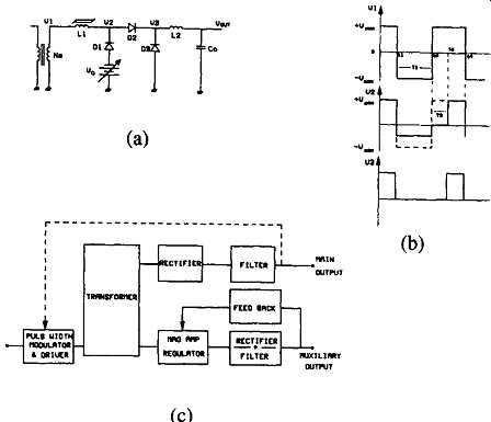

FGR. 11 Magnetic amplifier (a) Basic operation (b) waveforms (c) Two
output forward converter with mag amp (d) Mag amp control using UC 1838
(Reproduced with per mission of Unitrode Inc., USA) (e) Associated waveforms
for two output forward converter
When t=t 2, V 1 switches back t o +Vmax, the mag amp now acts as an inductor and prevents the current from flowing, holding V 2 at zero volts. This condition remains until the voltage across the core (now +Vmax) back into saturation. The important fact is that this takes the same volt-second value of (Vmax-Vcont) T 1 that was put into core during reset. Therefore:
(Vm~ ' - Vcont)T , = Vm.x(t3 - t2) = Vma.T 2 (4.2)
This allows the V o value to be regulated by the pulse duration of the on time.
Fgr. 11 (c) shows how a mag amp interrelates in a two-output forward converter illustrating the contribution of each output to primary current. Also shown is the use of the UC 1838 IC from Unitrode as the mag amp control element in Fgr. 11 (d) and 4-11 (e) indicates the relevant waveforms.
In addition to regulating, mag amps must often provide current limiting of the individual output. In these cases the saturable reactor must withstand the entire volt second product of the input waveform. Thus, there are two categories of application: regulation only and shutdown.
Elias (1994) and Mammano and Mullet provide design details of mag amps.
Another recent approach (Unitrode Inc. 3/97 and 4/97) for regulating the individual secondary voltages is to use series connected MOSFETs together with secondary side post regulator ICs. Some of these new integrated circuits such as UCC 1583 from Unitrode Inc. are proposed as replacement for mag amp circuits.
4.3 Power Rectifiers for Switching Power Supplies
The switching power supply demands that power rectifier diodes must have low forward voltage drop, fast recovery characteristics, and adequate power handling capability. Ordinary PN junction diodes are not suited for switching applications, basically because of their slow recovery and low efficiency. Three types of rectifier diodes are commonly used in switching power supplies:
(a) High-efficiency fast recovery rectifiers (b) High-efficiency very fast rectifier (c) Schottky barrier rectifiers Fgr. 12 shows the typical forward characteristics of these diode types. It can be seen from the graphs that Schottky barrier rectifiers exhibit the smallest for ward voltage drop and therefore provide higher efficiencies. Another newer device family is the GaAs power diodes discussed in Section 2.
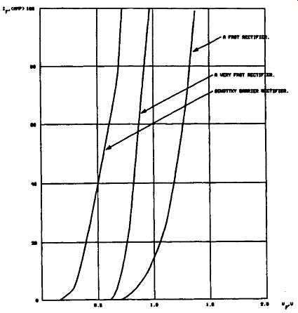
FGR. 12 Typical forward voltage drop characteristics of different rectifier
types
4.3.1 Fast and Very Fast Recovery Diodes
Fast and very fast recovery diodes have moderate to high forward voltage drop, ranging from 0.8 to 1.2 V. Because of this and because of their normally high blocking voltage capabilities, these diodes are particularly suited for low-power, auxiliary voltage rectification for outputs above 12 V.
Because most of today's power supplies operate much above 20KHz, the fast and very fast recovery diodes offer reduced reverse recovery time tRR in the nanosecond region for some types. Usually the rule of thumb is to select a fast recovery diode which will have a tRR value at least three times lower than the switching transistor rise time.
These types of diodes also reduce the switching spikes that are associated with the output ripple voltage. Although "soft" recovery diodes tend to be less noisy, their longer tRR and their higher reverse current IRM create much higher switching losses. Fgr. 13 shows the reverse recovery characteristics of abrupt and soft recovery type diodes.
Fast and very fast switching diodes used in switchmode power supplies as output rectifiers may or may not require heat sinking for their operation, depending upon the maximum working power in the intended application. Normally these diodes have very high junction temperatures, about 175°C, and most manufacturers give specification graphs, which will allow the designer to calculate the maximum output working current versus lead or case temperature.
For example, a new fast recovery diode family with 600V, 15A capabilities termed ultra Fast Recovery Epitaxial Diode (FRED) from International Rectifier exhibits extremely fast reverse recovery times, very low reverse recovery current, unusually "soft" recovery characteristics, and guaranteed avalanche.
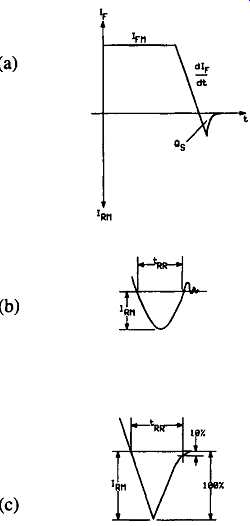
FGR. 13 Behavior of a rectifier as it’s switched from forward conduction
to reverse at a specific ramp rate dlr (a) Basic behavior of switching
(b) Abrupt recovery type (c) Soft recovery type dt
4.3.2 Schottky Barrier Rectifiers
The graph in Fgr. 12 reveals that the Schottky barrier rectifier has an extremely low forward voltage drop of about 0.5V, even at high forward currents.
This fact makes the Schottky rectifier particularly effective in low voltage outputs, such as 5V, since in general these outputs deliver high load currents. Moreover, as junction temperature increases in a Schottky, the forward voltage drop becomes even lower. Reverse recovery time in a Schottky rectifier is negligible, because this device is a majority-carrier semiconductor and therefore there is no minority-carrier storage charge to be removed during switching.
Unfortunately, there are two major drawbacks associated with Schottky barrier rectifiers. First, their reverse blocking capability is low, at present time approximately 100V to 150V. Second, their higher reverse leakage current makes them more susceptible to thermal runaway than other rectifier types. These problems can be averted, however, by providing transient overvoltage protection and by conservative selection of operating junction temperature.
4.3.3 Transient Over-Voltage Suppression
Consider the full-wave rectifier, shown in Fgr. 10(c) using Schottky rectifiers D1 and D2 in a PWM regulated half-bridge power supply. The voltage Vs across each half of the transformer secondary is 2 Vout minimum; therefore each diode must be capable of blocking 2 Vs at turn-off, or 4 Vout .
Unfortunately, the leakage inductance of the high-frequency transformer and the junction capacitance of the Schottky rectifier form a tuned circuit at turn-off, which introduces transient overvoltage ringing, as shown in Figure 14. The amplitude of this tinging may be high enough to exceed the blocking capabilities of the Schottky rectifiers, driving them to destruction during the turn-off period.
The addition of RC snubber networks will suppress this tinging to a safe amplitude, as shown in the lower waveform of Fgr. 14. There are two ways of incorporating RC snubbers at the output of a power supply to protect the Schottky rectifiers. For high current outputs the snubbers are placed across each rectifier as shown in Fgr. 15(a) while for low current outputs a single RC snubber across the transformer secondary winding, as shown in Fgr. 15(b) may be adequate.
Another solution is to place a zener diode, as shown in Fgr. 15(c) to clamp the excessive voltage overshoot to safe levels. Although this method works well, the slow recovery of a zener may induce noise spikes at the power supply out put which may not be desirable for low noise applications. For calculation details of RC components of snubber circuits Chryssis (1989) is suggested.
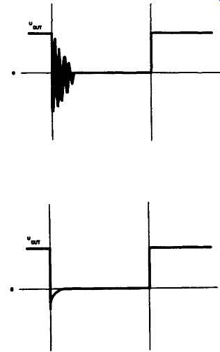
FGR. 14 Ringing during Schottky rectifier turn-off (a) With no snubber
(b) With snubber
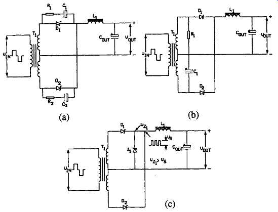
FGR. 15 Means of protecting output Schottky rectifiers during turn-off
(a) Snubbers placed across each rectifier (b) A single RC snubber placed
across the transformer (c) Using a zener diode
4.3.4 Synchronous Rectifiers
As digital integrated circuit manufacturers are working toward implementing more electrical functions and circuits on a single silicon chip, the need for lower bias voltages becomes evident. For example, there are new families of logic circuits which require 3.3V supply.
These new voltage standards have forced design engineers of switching power supplies to explore the possibility of using devices other than junction diodes for rectification, in order to reduce the power losses encountered at the output section.
Since the power dissipation is directly proportional to the diode's forward voltage drop, even the best Schottky rectifiers with a 0.4V forward voltage drop may account for up to 20 percent of the total input power loss.
In recent years the power semiconductors such as bipolar power transistors and power MOSFETS have provided an alternative in power rectification and these devices working as synchronous rectifiers have started to appear in switching power supply designs. Use of ultra-low rDs,(on ) MOSFETs as synchronous rectifiers may provide the best solution for overcoming the single most important barrier to higher power supply efficiency.
Low rDs,(on ) MOSFETs employ VLSI processing and design techniques that allow manufacture of low-voltage MOSFETs with more parallel cells packed into given die area. The result is a reduced channel resistance, which is the dominant component of rDs,(on ) for devices with breakdown voltages under 60 V. For example, a process developed by Siliconix Inc., USA enables 2.5 million MOSFET cells per square inch of die with good manufacturing yields. This process allows manufacturing economical MOSFETs with 18 mf~ maximum on resistance in a TO-220 package.
4.3.4.1 Practical Circuit Configurations
Fgr. 16 shows a practical implementation of a center-tapped full-wave output section of a switching power supply utilizing power MOSFETs as synchro nous rectifiers.
MOSFETs QI and Q2 are selected to have minimum possible RDS,(on ) at maximum output current, in order to increase efficiency. Transformer windings N 3 and N 4 are used to turn on the MOSFETs at opposite half cycles of the input waveform.
It’s beneficial to overdrive the gate-to-source voltage in order to minimize RDS,(on ).
Careful selection of resistors R 1 through R 4 will also minimize the switching times. Diodes D 1 and D 2 are parasitic diodes of the MOSFETs, and act as free wheeling diodes during the input wave-form dead time t d to provide current path for inductor L 1.
Fgr. 17 shows the implementation of the MOSFET as synchronous rectifier in a single-ended forward converter. In this configuration transistor Q I turns on by the gate-to-source voltage developed by winding N 1, on the positive cycle of the switching waveform. When the input voltage swings negative, MOSFET Q I turns off and output current is supplied to the load through MOSFET Q2, which now turns on through coupled winding N 3 using energy stored in the output inductor L.
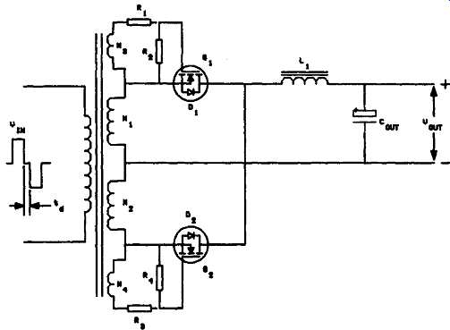
FGR. 16 Full-wave output rectification of a switching power supply using
MOS FETS as synchronous rectifiers
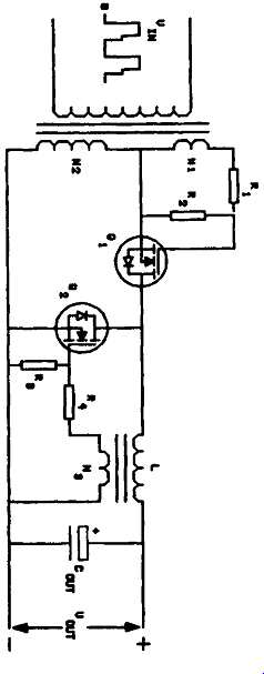
FGR. 17 Circuit implementation of a forward converter output section using
power MOSFETS as synchronous rectifiers.
The criteria for choosing the proper MOSFET parameters for use in this circuit are the same as in the bridge configuration output circuit.
Synchronous rectifiers implemented with special bipolar transistors offer all the advantages of the MOSFET synchronous rectifiers up to frequencies of 200 KHz (above this frequency the MOSFET dominates), coupled with lower prices and improve temperature coefficients compared to power MOSFETs. For details of practical implementation of bipolar synchronous rectifiers Chryssis (1989) is suggested.
4.4 Inductors and Capacitors in the Output Section
4.4.1 Inductors and Capacitors: A Comparison
Inductors and capacitors are used in the output section as energy storage elements. Table 4-5 is a comparison of some capacitors and inductors to store the energy of 0.1 joule. The data is based on information as per Persson (1994) prices.
Data may vary depending on selections. Using this table as a guideline one could easily see that inductors are bulky, costly, and heavy. However for the reasons given below inductors and capacitors can not be just interchanged.
a. Capacitors behave like low impedance voltage sources
b. Inductors behave like high impedance current sources Most switching power supply designs use an inductor as part of their output filtering configuration. The purpose of this inductor is two-fold. First, it stores energy during the off or "notch" periods in order to keep the output current flowing continuously to the load. Second, it aids to smooth out and average the output volt age tipple to acceptable levels.
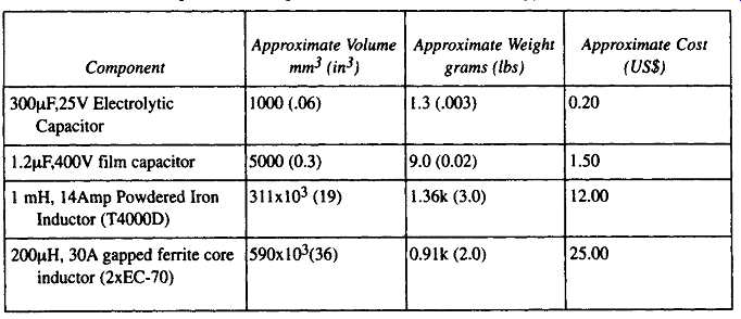
TABLE 5 Comparison of Capacitors and Inductors as Energy Storage Elements
Component
300p.E25V Electrolytic Capacitor
1.2~tE400V film capacitor
1 mH, 14Amp Powdered Iron Inductor (T4000D) 200~tH, 30A gapped ferrite core inductor (2xEC-70)
Approximate Volume
Mm^3 (in^3 )
1000 (.06) 5000 (0.3) 311x103 (19) 590x103(36) grams (lbs) Approximate Weight Approximate Cost (us$) 1.3 (.003) 9.0 (0.02) 1.36k (3.0) 0.20 1.50 12.00 25.00 0.91k (2.0)
===
4.4.2 Output Filter Capacitors
Ripple falter capacitors are major factors in reducing the size and weight of power conversion systems. Typical capacitors for this application include tantalums, electrolytics, multilayer ceramic (MLC), and the Multi-layer Polymer (MLP) capacitors.
Two of the most important high frequency SMPS capacitor characteristics are equivalent series resistance, ESR, and equivalent series inductance, ESI. These two parameters affect the output tipple voltage, output noise, and supply efficiency.
When SMPS technology was in its infancy, no single output capacitor could meet low ESR requirements, so several capacitors were used in parallel to meet tipple current specifications.
Output filters in high frequency SMPS units require extremely low ESR and ESL capacitors. These requirements are beyond the practical limits of electrolytic capacitors, both aluminum and tantalum. However, MLC and MLP capacitors meet these requirements.
At high switching frequencies, filter inductance or ESL dominates output ripple voltage. MLC output filter capacitors have ESR and ESL values well below the minimum values needed resulting in lower noise levels at high frequencies, thus eliminating the need for parallel output filter capacitors. Currently, one of the driving forces for size reduction in higher frequency supplies is use of surface mount technology (SMT). MLCs are compatible with SMT reflow and assembly techniques.
Much newer process techniques used in the MLP capacitors, offer excellent electrical stability under AC and DC loads and are not subject to the cracking, shorting, or temperature coefficient mismatches inherent in MLC types (Clelland and Price 1994). The MLP capacitor is fully surface mount compatible and is best described as a construction hybrid between MLC and stacked, plastic film capacitors.
The present offering of non-polar, highly stable MLP capacitors covers the range from 0.00471aF through 201aF with voltages from 25 to 500 VDC. Today, this technology is leading in C * V density and is growing most rapidly in input voltage filtering from 48 to 400V, and output filtering at 24 to 48V. Many of the products are available in surface mount styles as either lead-framed construction or as true "chip" capacitors. Some of the commercially available MLP capacitor ranges are Angstor, Surfilm, and Capstick. Table 4--6 indicates the applications, and ranges applicable in these MLP capacitors.
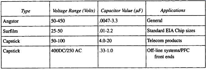
TABLE 6 MLP Capacitors and Applications (Source: Clelland and Price 1994)
Angstor Surfilm Capstick Capstick
Type Voltage Range (Volts) Capacitor Value (t~F)
Applications
50-450 .0047-3.3 General 25-50 .01-2.2 Standard EtA Chip sizes 50-100 4.0-20 Telecom products 400DC/250 AC .33-1.0 Off-line systems/PFC front ends
For further details on MLC and MLP capacitors references Clelland (1992), Lienemann (1992), Clelland and Price (1993, 1994, 1997), and Cygan (1997) are suggested.
5. Ancillary, Supervisory, and Peripheral Circuits
In general, switching power supplies are closed-loop systems, a necessity for good regulation, ripple reduction, and system stability. Other than the basic building blocks, which have been described in the previous sections, there are a number of peripheral and ancillary circuits that enhance the performance and reliability of the power supply.
Components such as opto-isolators are extensively used in the flyback or feed-forward converter to offer the necessary input-to-output isolation and still maintain good signal transfer information. Other circuits, such as soft-start, over current, and overvoltage protection circuits, are used to guard the power supply against failures due to external stresses. The details of such circuits and components are beyond the scope of a section of this kind.
6. Power Supplies for Computers
In today's electronics marketplace, power supply vendors face a tremendous market for the various power supplies required by computer systems. For the most popular models of portable, desktop, and minicomputer systems, manufacturers demand regulated power supplies with direct AC line operation with output capacities of approximately 25 to 500W; multiple low DC voltage of 5V, 12V, -12V, and -5V derived from the same ferrite transformer with multiple secondary windings;
individual regulation using three terminal regulators; monolithic primary side controller chips to switch the DC voltage across the ferrite transformer to provide the necessary isolation from the low-voltage output; RFI and EMI filters installed at the incoming end of the AC supply t o prevent high-frequency pollution generated by the SMPS; and the various supervisory and control circuits required for reliable SMPS operation.
In most computer power supplies (Fgr. 18) multiple outputs are under the control of a single SMPS controller chip. Depending on the power output, various auxiliary circuits may be powered from independent SMPS modules or linear blocks, especially in high capability minicomputer power supplies.
The latest microprocessors to emerge from Intel, Motorola, and others are forcing fundamental changes in the power supplies for desktop and portable computers. But not only do the laps demand lower and more precise supply voltages, but their main clocks also exhibit start/stop operation that causes ultra-fast load transients. As a result, the relatively simple 5V/12V supply has been transformed into a system with five or more outputs, featuring unprecedented accuracy and 50A/las load-current slew rates.
These characteristics present a problem: it appears that the classic, centralized power-supply architecture cannot provide the accuracy and transient response needed by coming generations of computer systems. The more effective approach will be a distributed architecture in which local, highly efficient DC-DC converters are located on the mother board next to the CPU.
Product designers could expect power-supply manufacturers to respond with smaller, higher-frequency ICs and modules that feature improved dynamic response and better synchronous rectifiers. The PC's off-line power supply won’t disappear.
It will remain to generate the main bus for small DC-DC converters on the mother board.
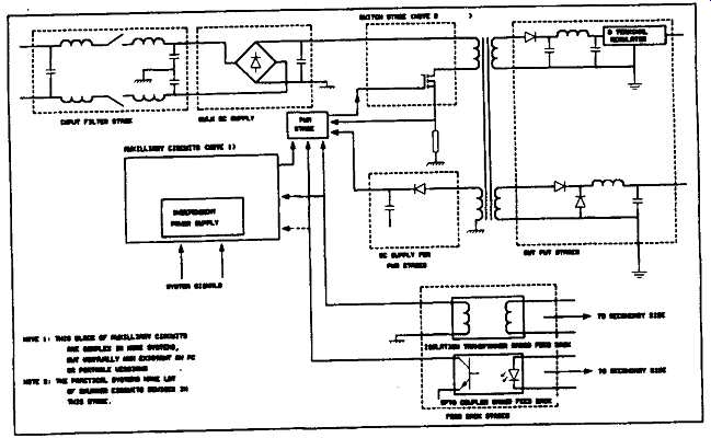
Above: Fig. 18 A representative computer power supply
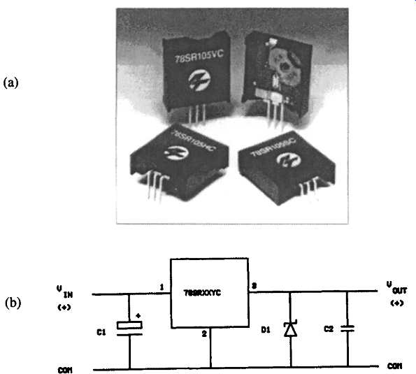
Above: Fig. 19 Integrated switching regulator modules (Power Trends
Inc., USA.) (a) 3 terminal modules (b) A typical application
7. Modular SMPS Units for Various Industrial Systems
With a heavy demand from industrial system designers for different series of low-power (less than 100W) and low-voltage power supply blocks, many manufacturers have introduced various kinds of DC/DC converter modules for various fixed output voltages such as 5V, _12V, ±15V, 24V, 28V, and ±48V for off-the-shelf selection. The same manufacturers market similar AC/DC power supply modules, among them the manufacturers such as Vicor, Lambda, Kepco, and Datel.
Another new series of devices coming to the market are integrated switching regulators. Units such as those by Power Trends (Fgr. 19) are similar to the popular three-terminal linear voltage regulators.
One recent advancement was to move power MOSFET from its discrete pack age and heat sink on to the same silicon die as its controller, building a power IC.
With this new trend, designs could minimize the total component count of an off the-line SMPS. Power switches and the controller packaged in one IC could be used with few other external magnetic components and the feedback loop requirements.
Classic examples of these are the TOP switch series from Power Integration and VIPer 100 series from SGS Thompson. These switchers offer power outputs in the 10 to 150W range, which is sufficient for modem desktop PCs and similar applications.
TOP switches are available for universal wide-input-range applications such as 85 to 260V or 110/115/230V AC inputs. Similarly the VIP (Vertical Integrated Power) family, which is a 600V rated component, could operate from a rectified 85/115V AC line. These components, operating at lower frequencies (100 to 200 kHz), could virtually eliminate EMI/RFI problems too. For details Goodenough (1997) is suggested.
8. Future Trends in SMPS
In this decade, power conversion designs will lead towards decentralized distributed systems. Technically, this will create a situation in which power-hungry systems will contain one central DC power supply distributed to all subassemblies of PCBs with local SMPS units powering the circuitry. Four key factors listed below are dictating the move toward distributed power.
• Central power supplies no longer support the advanced semiconductors that operate at lower supply voltages, run at greater speeds and demand more power.
• Custom power supplies require a long development cycle and are costly.
• Distributed power with parallel modules are more adaptable to design standards.
• Redundancy with parallel modules permits improved reliability, easy maintenance and on-line repair.
• Distributed power supplies can be made using surface-mount technology (SMT) components to support automated manufacturing.
With the move towards distributed power, several trends and changes affect the design and application of power supplies, including" greater power density (switching frequency and efficiency); resonant conversion techniques (surface mount, hybrid construction, and automated assembly); low-profile magnetics; changes in extra-low voltage safety requirements (such as the International Electro Technical Commission changing the Safety Extra Low Voltage (SELV) limits from DC 42.4V to 60V); and the development of DC uninterruptible power supplies.
An important technical requirement of future switched-mode power supplies will be the power factor correction that will be mandatory above a certain power consumption limit, such as 700 VA. This is because of the inherent characteristic of switch-modes, where the input current waveforms from AC line will be non-sinusoidal (and pulsed) and the peak of the current waveform and the peak AC input voltage won’t coincide. To meet such requirements, several companies produce power factor controller chips such as Micro Linear's ML4812 and ML4813 that help to achieve a nearly unity power factor SMPS. Kularatna (1992) and Maxim Inc. (1995) provide a detailed account of future trends.
9. Field Trouble-Shooting of Computer Systems Power Supplies
In environments where power quality on the commercial AC lines is not up to standards, such as in some developing countries, a large percentage (perhaps 25 per cent) of hardware faults on mini, micro, and portable computers occur in the power supplies. To begin with a fault trace procedure, the input stage that carries the AC power into the bulk DC stage (via an RFI/EMI filter) should be checked for the availability of AC line voltage after the filter stage (following a careful visual inspection for physically damaged power components).
If this stage is found to be fault-free, the next step is to check the bulk DC stage where reasonably high DC voltages (up to 350V in cases of AC 220V, 50Hz inputs) are present. An oscilloscope should be used to make sure that an excessive ripple component is not present, superimposed on the bulk DC.
Once troubleshooting has confirmed the availability of bulk DC, the next step is to check the PWM controllers, using circuit diagrams to identify the topology of the switching stage and the type of power semiconductors used for switching. In most computer power supplies a large number of snubbers and clamping circuits (based on RC components or zener diodes) etc. are used around the drive stages for reducing the transients below the maximum ratings of power semiconductors.
It’s always safe and saves time to check the correct operation of zener diodes or other semiconductor devices around the drive circuits and the main power elements before using the scope to check the drive pulses. In many cases of power transistor failures, several other semiconductors around the power transistors also may be faulty.
If the main power semiconductors are operational and drive pulses are avail able, the voltage- or current-related feedback paths should be checked. In cases where the pulses driving the main switch elements are not observed, the feedback operation of the SMPS controller chips should be checked. In most cases, the out put voltage feedback signal is derived from the output power rail that drives the maximum VA rating. In a personal computer power supply, most power is drawn from the 5V rail.
In cases where none of the output voltages are present, it might be worth suspecting the primary side of the SMPS rather than placing priority on the individual regulators and other associated circuitry on the output power rails. In the case of complex minicomputer power supplies, there may be many control inputs coming from the auxiliary circuits which act as safety measures to stop or regulate the over all system. In such cases, it may be necessary to identify those areas and signals that may be inhibiting the final drives.
Once the primary side oscillation is achieved, most of the basic trouble-shooting is achieved. When one or two output rails have their specified voltages, it’s a matter of detailing the secondary side for individual rail faults. In practice, a dummy load may need be connected to the 5V output in case intermittent oscillations or unregulated outputs are observed.