AMAZON multi-meters discounts AMAZON oscilloscope discounts
1. Scope
The primary function of a power supply is to draw electrical power from an existing electrical system and convert this power into a form suitable for a particular load. A wide variety of power supplies is used to meet the range of loads presented by common electrical equipment. This Section covers the common power conversion circuits that use semiconductor switches. These are commonly known as static power supplies, and the overall requirements which influence their design and construction are described here. Systems that use rotating machines or which control the flow of power using metal-contact switches have been common in the past but are increasingly restricted to specialized applications; they are not covered.
The power that is handled by static power supplies can range from a few milliwatts, supplying low-voltage integrated circuits, to gigawatts in high-voltage dc links. This Section concentrates on equipment of less than a few tens of kilowatts drawing ac power from a standard utility supply; this represents the majority of static power supplies manufactured and in use today.
2. General issues
2.1 Design optimization
The majority of static power supplies are manufactured to compete in markets where the purchase price is often the primary concern of the customer, given a minimum electrical specification and a basic level of reliability.
Other features such as size, weight, efficiency and acoustic noise are often secondary issues, although in some battery-charging applications efficiency may be critical and in aircraft weight is of paramount imp0rtan.e.
2.2 Thermal management
In static power supplies a significant proportion of the input power is dissipated as heat, and adequate cooling must be provided in order to limit the temperatures reached by the circuit components and to avoid damaging them. A maximum ambient temperature of 40°C to 60°C is often specified, and safe component temperatures must be maintained in these conditions. Component temperatures may be up to 70°C for resistors, 85°C or 105 C for capacitors, 90°C to 110°C for heat sinks, 100°C for wound components (inductors and transformers) and 120°C for power semiconductors.
At the lowest power levels, heat is removed from the components by natural convection and radiation. At higher power levels fan cooling is used, air speeds being typically in the range 0.5 to 5 m/s. Liquid cooling is normally used at much higher power levels than 10 to 20 kW.
2.3 Safety
Voltages in static power supplies are often at lethal levels (in excess of 55 V relative to earth). Prevention from electrocution is therefore necessary. Measures which are used to meet the requirements set down in standards are: the use of earthed metal enclosures in which any openings are below a specified size the referencing of output voltages to earth, which often requires the use of an isolation transformer design so that the insulation materials used to achieve safety isolation are maintained within their rated maximum temperatures Protection against fire is also an important consideration and an input fuse is used to prevent sustained overheating and fire in the case of component failure.
2.4 Compatibility
Static power supplies must deal with various levels of disturbance in the utility supply (or other supplies such as standby generators and systems powered by renewable energy sources) and still maintain the required output to the load. The main disturbances to the utility supply which must be dealt with are: blackout (outage) - absence of utility supply for a cycle or more; this is often due to faults on the electrical supply system, and the operation of system protection equipment brownout (sags) - the utility supply voltage falls below the normal minimum rms level for more than one cycle. This is often due to the switching on of large loads on the utility system overvoltage--the utility supply voltage rises above the normal maximum rms level for more than one cycle; this is often due to the switching off of large loads on the utility system voltage spikes--high voltages of short duration, superimposed on the utility supply waveform; this is often caused by switching of inductive loads or by lightning strikes in the utility system harmonic currents--distortion of the sinusoidal supply waveform; this is due to harmonic currents (for instance from rectifiers, dc-dc converters and arc welding) flowing through the utility system impedances Radio Frequency Interference (RFI)--these arise typically from high-speed switching transients and from arc welding Filters are commonly used at the input stage of static power supplies to protect against or limit the effect of these disturbances, and uninterruptible power supplies are used to protect against blackouts and brownouts.
2.5 Commissioning, testing, installation and maintenance
Commissioning of static power supplies is usually necessary only for equipment which is rated at tens of kilowatts or more. Below this power level, in the range which this Section addresses, equipment is normally fully tested and set up by the manufacturer before dispatch to the customer.
3. Supply-frequency diode rectifiers
Rectifiers convert ac to dc. Full-wave and half-wave rectifier circuits are available for both single-phase and three-phase utility supplies, and the choice usually depends upon the power to be delivered to the dc load.
The diodes used in rectifiers are often integrated into one component, which may be mounted on a heat sink. The need for a suitable safety margin often results in the use of 800 V-rated diodes for 230 V single-phase direct off-line power supplies, and 1200 V rating for 415 V three-phase direct off-line applications.
High-frequency filter capacitors are often connected in parallel with rectifier diodes. These capacitors protect the diodes from transient voltage spikes by acting as a low-impedance path to high-frequency voltages.
It is common to obtain the required output voltage using a transformer which is connected between the ac supply input and the rectifier. The use of an isolating transformer not only allows the output voltage to be set, but by isolating the rectifier circuit from the ac supply it also enables one dc output voltage rail to be referenced to earth. The earthing of a low-voltage output connection is necessary in many applications in order to prevent injury by electrocution.
3.1 Half-wave single-phase rectifiers
For low power levels, a single-phase half-wave circuit with a large dc output capacitor to reduce voltage ripple is normally used. The circuit is shown in Fig. 1. When the ac supply voltage Vs(t) exceeds the voltage V,(t) at the output of the rectifier, the voltage difference causes a supply current id(t) to flow. The rate of rise of this current is limited mainly by the supply inductance Ls. As the capacitance C is charged, VL(t) rises. When the supply voltage Vs(t) decreases after passing its peak, it falls below VL(r) and the supply current id(r) falls to zero. During the period when idt) is zero, VL(t) falls as the capacitor discharges. The decay in this voltage is approximately linear. but it will be exponential if the load is resistive and falls with an increasing rate when supplying constant power to a switching regulator.
When the circuit is first energized, the capacitor is initially fully discharged and there is a large surge of supply current as it is charged. To limit this surge to an acceptable level, thermistors with a negative temperature coefficient are often connected in the ac circuit. The resistance of the thermistor is initially high and the current is limited by this to the required level, but after a short period of conduction the thermistor temperature rises and its resistance drops, reducing the power loss and voltage drop in normal operation. This thermal characteristic requires a minimum time between the ac supply being switched off and reconnected in order that the thermistor temperature can fall sufficiently to limit the surge current on reconnection to an acceptable level. For applications requiring maximum efficiency, the thermistor may be replaced by a resistor connected in parallel with a relay contact or a semiconductor switch which closes after the initial charging surge.
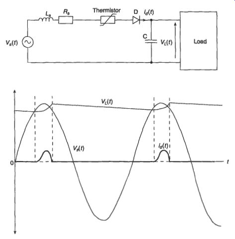
Fig. 1 Half-wave single-phase rectifier
3.2 Full-wave single-phase rectifiers
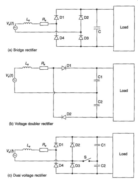
Fig. 2 Full-wave single-phase rectifiers ---(a) Bridge rectifier (b); (c)
Dual voltage rectifier
The three main circuits used are illustrated in Fig. 2.
The bridge rectifier circuit in Fig. 2(a) allows current to flow through diodes D1 and D3 when the supply voltage V() exceeds the load voltage, and through D2 and D4 when V,(t) is more negative than the load voltage is positive. Supply current therefore flows in both polarities. Ideally this avoids a dc component of supply current and reduces the peak supply current levels. The rectifier delivers power during each half-cycle of the ac supply and this reduces the size of the capacitor required to limit the output voltage ripple.
The voltage-doubler rectifier shown in Fig. 2(b) can be regarded as two half- wave rectifiers, with D1 conducting during positive half-cycles of the ac supply and D2 conducting during negative half-cycles.
The dual-voltage rectifier of Fig. 2(c) has a link S which can be used to configure the rectifier as a bridge or as a voltage doubler. This arrangement is commonly used to deliver approximately the same dc voltage using either bridge rectification of 230 V ac or voltage-doubler rectification of 110 V ac. In this way, by changing the link S, the rectifier can be configured for use in most countries.
3.3 Three-phase bridge rectifiers
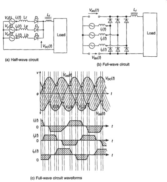
Fig. 3 Three-phase diode rectifiers -----(a) Half-wave circuit; (b) Full-wave
circuit; (c) Full-wave circuit waveforms
Three-phase bridge rectifiers are typically used above 1 kW to provide a single dc supply by rectifying the line-to-line voltage. The scheme is illustrated in Fig. 3(b). For completeness Fig. 3(a) shows the half-wave circuit, but this is not commonly used. The bridge rectifier produces six pulses of power near the peaks of the line-to- line voltages. It is common for the load of a three-phase rectifier to include a large inductance (shown as LJ) to create a dc current source. Figure 11.3(c) shows typical waveforms and it illustrates the time required for the supply current to rise and fall from the level of rectifier output current.
For high power outputs, two three-phase supplies are used. These have a phase difference of 30 degrees and the supply is rectified to provide 12 pulses per cycle. A center-tapped inductor is connected between the negative dc outputs of the two six-pulse rectifiers, and the negative supply to the load is connected from the center tap of this inductor in order to limit sixth harmonic (300 Hz) currents. The main advantage of 12-pulse, compared with six-pulse, rectifiers is that the filtering requirements are reduced; the primary current waveforms have no fifth or seventh harmonic components, which reduce the filtering required in the ac supply, and the dc output has more pulses, which reduce the ripple contained in the dc output.
3.4 Voltage multipliers
These are rectifier circuits in which diodes and capacitors are used to deliver an output voltage which is an integral multiple of the peak ac input voltage. Different circuits are possible and a voltage doubler has already been shown in Fig. 2(b). A common circuit is shown in Fig. 4 and the operation is: C1 charges to the negative peak supply voltage through D1 when the ac source reverses, the voltage across C1 adds to the source voltage, and C2 is charged through D2 to twice the peak source voltage C3 and C4 charge in a similar way to C1 and C2, except that both these capacitors charge to twice the peak ac voltage
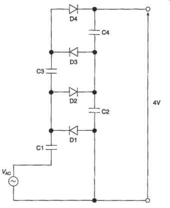
Fig. 4 Voltage multiplier
Further stages can be added to increase the output voltage, although the output voltage will not be the full multiple of the input voltage because of voltage drops in the components.
Voltage multipliers are suited to low-current high-voltage supplies, and they are rarely used for supplying more than a few milliamps.
4. Phase-controlled power converters
Phase-controlled power converters use thyristors, which begin to conduct when turned on by a gate signal. If the load current exceeds a latching current level, a thyristor will latch in the conducting state and it will continue to conduct, irrespective of the gate signal. When the load current falls below a relatively small 'holding current' the latching action will stop and the thyristor will turn off provided the gate signal is in the off state. Power flow is controlled by timing the instant of turn-on of the thyristor to a set phase angle in the ac waveform.
Detection of ac supply zero-voltage crossings is used to ensure that the thyristor control signals are timed in correct phase with the supply voltage waveform. A ramp and a dc control voltage are taken as input to a comparator, which delivers an 'enable' signal to an oscillator. The oscillator output is amplified and passed through a pulse transformer (for electrical isolation) and through a current-limiting resistor to the thyristor terminals. A train of pulses is applied between gate and cathode terminals of the thyristor to minimize the size of the isolation transformer whilst ensuring that the thyristor cannot turn off for long during the conduction period set by the control circuit.
The switching of thyristors often requires snubbers. These prevent damage to the thyristors by limiting overvoltages, the rate of rise of voltage across the thyristor and the rate of change of thyristor current. A wide variety of snubber circuits are commonly used.
4.1 AC power controllers
Circuits for the control of single-phase ac power using phase-controlled thyristors are illustrated in Fig. 5. Anti-parallel thyristors (Fig. 5(c)), or a thyristor with an anti-parallel diode (Fig. 5(b)), or simply a triac (Fig. 5(a)) can be used.
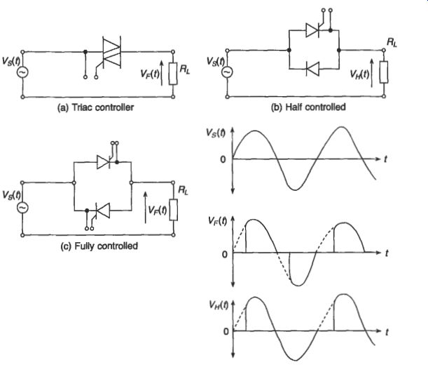
Fig. 5 Single-phase phase-controlled ac regulators ---(a) Triac controller
; (b) Half controlled ; (c) Fully controlled
The resulting current waveform depends upon the load impedance, which is often resistive, for instance in the case of dimmers used for incandescent lights.
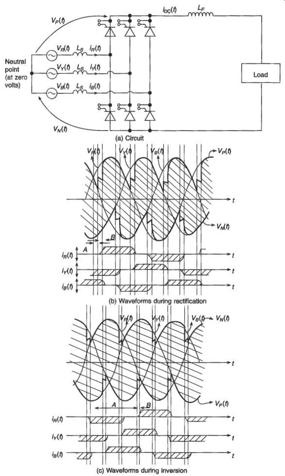
Fig. 6 Three-phase phase-controlled rectified inverter -- (c) Waveforms
during inversion.
4.2 Phase-controlled rectifiers and inverters
A phase-controlled inverter uses the same circuitry as a phase-controlled rectifier, but with a different timing for the thyristor drive signal. The circuit is shown in Fig. 6(a). The basic three-phase bridge arrangement is similar to that used in the diode rectifier circuit already seen in Fig. 3(b); the main difference is that using the thyristors, the start of current conduction can be delayed for a controlled period after the zero-voltage crossing of the anode-to-cathode voltage.
Phase-controlled rectifiers and inverters are normally used at high power levels with three-phase supplies. A large inductance Lf is connected in series with the dc output in order to ensure a substantially ripple-free dc current.
The waveforms in a three-phase rectifier with constant-current output are shown in Fig. 6(b). The conduction of each thyristor is delayed beyond the instant that a diode would conduct by a delay angle A. When conduction has begun, the rectifier output takes a time, represented by angle B to commutate from the previously conducting phase. This is illustrated by the gradual decay in the outgoing phase current i&) and the corresponding rise in the incoming phase current it@).
5. Linear dc voltage regulators
Linear regulators use a bipolar transistor connected in series with the load, and operating in the linear mode, in order to regulate the load voltage by controlling the transistor voltage drop. Basic schemes are shown in Fig. 7.
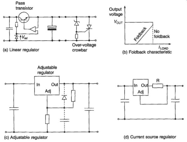
Fig. 7 Linear regulator schemes
Linear regulators are often implemented in a single three-terminal Integrated Circuit (IC), which requires only the connection of input and output decoupling capacitors and mounting on a heat sink. Fixed output voltages at standard values are delivered by regulators such as the 78xx series of positive voltage regulators and the 79XX series of negative voltage regulators. These regulator ICs usually contain additional features such as overtemperature and overcurrent protection circuits.
In cases where the heat dissipation in the internal pass transistor is high, a separate transistor is often used instead of an IC. This enables the control circuits to operate at an acceptably lower temperature while allowing a high temperature in the pass transistor itself. In such applications, the dissipation in the pass transistor, which is proportional to its voltage drop, is often minimized by the use o€ a 'low dropout' regulator. Standard linear regulators require the input voltage to be a minimum of 3 V higher than the output voltage for correct operation of the control circuitry. 'Low dropout' regulators operate satisfactorily with minimum voltage drop which may be less than 1 volt.
Output overvoltage protection is often used to safeguard the load. This protection works by short-circuiting the regulator output in the event of an overvoltage; the 'crowbar' for achieving this is shown in Fig. 7(a). The resulting short-circuit current operates either the current-limit protection within the regulator or the input fuse. If the load current were limited by the regulator to its maximum value, then the pass transistor would dissipate maximum power with the output short-circuited, when the voltage across the regulator is also a maximum. Such high power dissipation would usually exceed the maximum acceptable for normal operation, and it would increase the required cooling. To avoid the need for this increased cooling, the output current is often reduced (or 'folded back') in cases where the load impedance is less than the full load impedance. A foldback characteristic is shown in Fig. 7b. Adjustable regulators include an external resistive voltage divider to set the output voltage, as shown in Fig. 7(c). A common IC used in adjustable regulators is the LM317.
Micropower linear regulators for use in battery-powered systems are optimized for very low quiescent current (the current that supplies the regulator control circuitry). Dual-tracking regulators deliver equal positive and negative dc voltages. This is achieved by arranging that the pass transistor on the negative rail tracks the magnitude of the regulated output of the positive regulator.
6 Inverters Although phase-controlled inverters require an existing ac system into which their output is delivered, a variety of other inverter types are used in order to create an ac supply-frequency power source.
In some applications, a dc source may be inverted to a square wave output by the use of four transistors which connect the dc input to the load in alternating polarity at the required frequency. This type of system is simple, efficient and has low noise; it also enables the use of slow switches for low-frequency applications.
Resonant schemes apply a square wave at the required output frequency to a resonant circuit which may be connected in series, in parallel or in series-parallel.
The resonant circuit has a natural frequency which is equal to the required output frequency; it generates an approximate sine wave from the square wave, and acts as a low-impedance source.
Linear amplifiers are used to amplify a reference sine wave to the required ac output voltage, the output oscillating between positive and negative dc voltage rails.
The linear amplifier has a low source impedance, and it offers low noise generation because of the avoidance of switching transients, but there are high power losses in the amplifier transistors.
Pulse- Width Modulated (PWM) inverters use high-frequency switching of the dc source voltage, in which the pulse width is proportional to the ac waveform amplitude.
Typically, a full bridge of transistors is controlled in such a way that a sinusoidal output voltage is achieved once switching frequency components have been filtered out. In comparison with linear inverters, PWM types are small, have higher efficiency and cope well with non-linear loads, but they generate substantial high-frequency noise.
7. Switching dc voltage regulators (dc to dc converters)
DC to dc converters are widely used for the regulation of dc voltage, and they are used in Switched-Mode Power Supplies (SMPS). They are commonly treated as a single power converter, although isolated versions use a controlled inverter and a rectifier. The circuitry differs significantly from that used in AC supply-frequency power conversion.
Switching regulators use the duty cycle of a switch to regulate a voltage. The switch has low power loss because it alternates between an off-state, during which a negligible leakage current flows through the switch, and an on-state, during which the switch conduction voltage is low. The switched waveforms are averaged using low-pass filters which consist of capacitors and inductors. The size of these filter components reduces with increasing frequency, but the switching loss increases in proportion with frequency; typical commercial equipment operates at a switching frequency in the range 100-500 khz.
The two types which are commonly used without isolation are the buck converter and the boost converter. These are shown in Figs 8 and 9 respectively. The converters are said to operate in 'continuous mode' when the induction current iL(t) is continuous, and in the 'discontinuous mode' when the iL(t) falls to zero for a part of each cycle.
Buck converters deliver an output voltage which is less than the input voltage. The dc input is switched using S with a pulse width that is controlled in order that the average output voltage (filtered using the inductor L and capacitor C) has an accurately controlled dc value. Suitable ICs are available. These incorporate most of the components and simplify the design.
Boost converters deliver an output voltage which exceeds the input voltage. In this case the switch S connects inductor L across the supply voltage, ramping up the inductor current; when S is opened, the current is diverted through the diode D to the output, and the current is reduced linearly.
If electrical isolation between input and output is required, a wide variety of converters are possible. The introduction of a transformer into the circuit for electrical isolation creates a need to limit the dc magnetizing current in the transformer in order to minimize core saturation and avoid the consequent damage to components because of excessive currents. The most common types of circuit are the flyback converter and the buck converter: The flyback converter is used for low power levels and the buck converter is used generally for outputs higher than about 200 W, where the size and cost of the output capacitor in the fly back converter become prohibitive.
Circuits and waveforms for a typical flyback converter and a typical buck-derived forward converter are shown in Figs 10 and 11 respectively.
The flyback converter uses a coupled inductor and operates in a similar way to the boost converter. The inductor current is built up in the primary winding (is(t)) when the switch S conducts, and is forced to flow in the secondary winding (iD(t)) through the diode D when the switch is off.
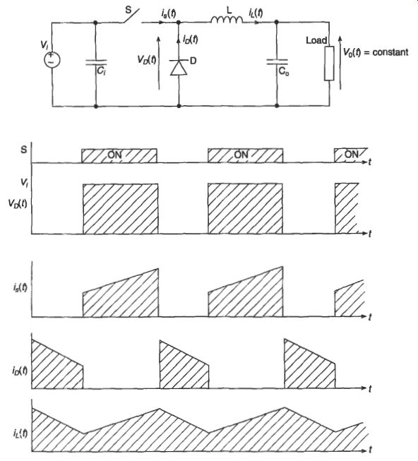
Fig. 8 Buck converter
The primary switches in the buck-derived converter invert the dc input voltage, and a PWM rectangular ac waveform V,(t) is applied to the primary winding of the isolation transformer. The secondary voltage is rectified by diodes D1 and D2 before being applied to the averaging filter which comprises inductor L and capacitor C. The output from the filter is a smoothed dc waveform with very little switching frequency ripple.
Stray inductances (mainly transformer leakage inductance) and stray capacitances (mainly in the switch and diodes) form resonant circuits which oscillate in response to switching transitions. These oscillations are damped in practical circuits by R-C snubbers which are connected across transformer windings and in parallel with diodes; the energy stored in stray and leakage inductances may be recovered using voltage clamps.
Auxiliary circuitry is necessary for the supply of power to the control circuit, for control circuit functions, to provide isolation in the feedback loop, and to drive power transistors.
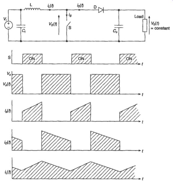
Fig. 9 Boost converter
8. AC supply harmonic filters
Filters are used to block and/or bypass selected frequency components of power circuit waveforms. Power circuit waveforms are usually composed of a dc component and an alternating component that is repeated each cycle. It can be shown that any repetitive waveform may be represented by the sum of a series of sinusoidal components, each of which has a frequency which is an integral multiple of the repetition frequency of the waveform. This series is known as the Fourier series. The component at the basic repetition frequency is known as the fundamental component, and other components are known as harmonics, the Nth harmonic having N times the frequency of the fundamental. The amplitudes of the harmonics generally decrease as their frequency increases. The representation of a square wave is shown in Fig. 12.
A filter incorporates inductors and capacitors, the impedance of which is proportional to frequency and inversely proportional to frequency respectively. These components are combined in a filter circuit to attenuate selectively the frequency components of the input waveform.
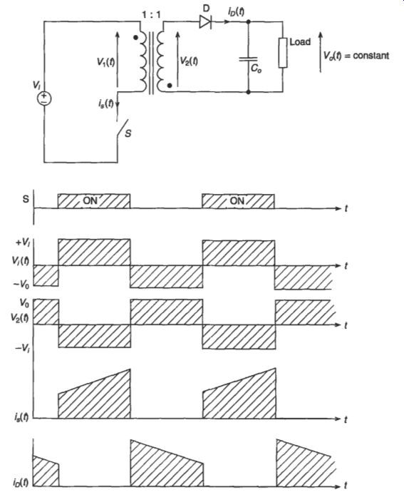
Fig. 10 Flyback converter
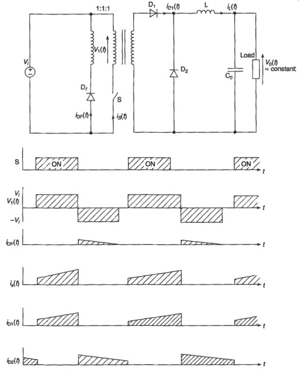
Fig. 11 Forward converter
8.1 Supply current harmonics
Loads which are connected to the utility supply may disrupt the operation of other loads by drawing harmonic currents from the network. Power supply rectifiers, which charge large capacitors, are a main source of harmonic current flow in the utility distribution system.
Distorted current waveforms affect other loads connected to the utility system because of the harmonic voltages which are developed across common impedances in the distribution network. Return currents flowing in single-phase neutral wires are added at the three-phase supply neutral point. If the load in the three phases is balanced, with unity power factor, then the neutral currents cancel exactly and zero neutral current flows. Typical neutral currents in rectifiers do not cancel, and the resulting neutral current, being the sum of the line currents, requires a higher-rated cable.
Three-phase rectifiers usually deliver dc output. Load current does not flow through the neutral wire and the input current waveform is usually acceptable without special measures to reduce harmonics.
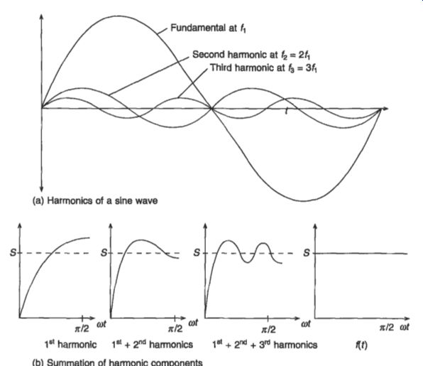
Fig. 12 Frequency components of a square wave.
8.2 The generation of current harmonics
In diode rectifiers, which are used to convert ac mains to a dc voltage source, the dc voltage ripple at the rectifier output is limited by a large capacitor. In the half-wave rectifier shown in Fig. 1, the dc capacitor C draws a pulse of current during the mains voltage peak. A full-wave rectifier as shown in Fig. 2 draws positive and negative pulses of current when the supply voltage is near its peak positive and negative values respectively.
The resulting supply current waveform is ac, and at the same fundamental frequency as the utility power supply, but it is not a pure sine wave. As previously explained, the waveform can be split into a Fourier series of pure sine wave frequencies which are harmonics of the fundamental frequency. The amplitudes of the harmonic components increase in magnitude if the pulse of current drawn by the capacitor is shorter; the pulse width depends upon the ac circuit impedance and the magnitude of the dc voltage ripple.
For a given dc voltage ripple requirement, which is set by the de capacitance value and the dc load current, the width of the supply current pulse can be increased by adding series inductance in the rectifier circuit, either in the ac connections or on the supply side of the dc capacitance. This method is considered to be acceptable at low power levels, but above about 400 W output the inductor becomes prohibitively large and preference is given to active methods which allow the use of a smaller inductor.
8.3 Current harmonics and power factor
Power factor has been defined in Section 2. Simply restated here, it is the total power taken from the supply divided by the ac supply voltage and the ac supply current. Reactive power flow and current waveform distortion reduce the power factor from its ideal value of unity.
Rectifiers delivering a dc voltage output usually draw little reactive current, but as pointed out above, they draw significant harmonic currents. The amount of distortion in the supply current waveform is usually quantified using the ac supply power factor, since reactive power flow can be neglected. Typical single-phase full-wave rectifiers of the type described above have a power factor in the region of 0.65 due to distortion of the current waveform.
8.4 Reduction of current harmonics
In order to attenuate the harmonic currents drawn by anon-linear load, an inductor may be connected in series with the load. This has the effect of reducing the load impedance variation, this variation being responsible for generating the harmonic currents.
Alternatively, a circuit or filter which provides a low-impedance path at a harmonic frequency may be connected into the supply side of the load in order to bypass most of the harmonic current. At high power levels, a series resonant circuit is used; this comprises an inductor and a capacitor which are tuned to &he harmonic frequency which is to be bypassed. In a 12-pulse inverter, for instance, a tuned filter is generally used to bypass the 11th and 13th harmonics and an LC filter is used for higher harmonics. Care is taken in the design of these filters to avoid high power loss at the fundamental frequency. Filters of this type are generally used in very high power applications such as HVDC transmission schemes.
Active power factor correction is often used in single-phase systems with a power output above about 400 W, where a passive system as described above would require an inductor of impractical size. Active power factor correction is usually based on a boost converter switching at a constant high frequency of 16 khz or above, and using PWM control to achieve approximately unity power factor. The high-frequency switching enables a relatively small inductance value to be used. A typical scheme is shown in Fig. 13. In comparison with a non-corrected system, active power factor correction provides the benefits of reduced dc voltage ripple, reduced dc bulk capacitance and reduced rms supply current. It can also enable a universal input by working with low-voltage ac supplies at higher line currents. These benefits do not compensate for the increased cost, complexity and power losses associated with active power factor correction, but supply harmonic limits may be enforced by law, and this would lead to its widespread use.
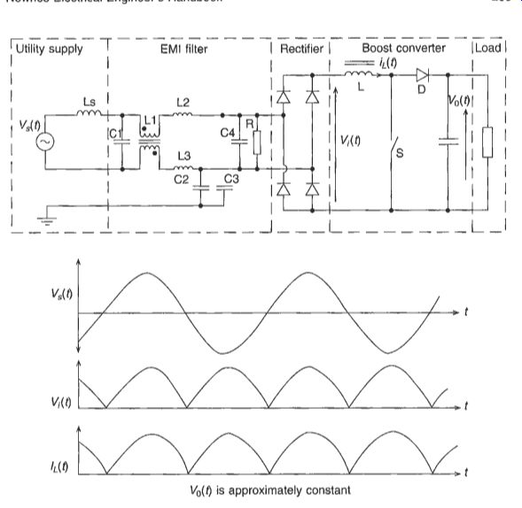
Fig. 13 Power factor correction boost converter
A PWM-controlled inverter, when connected to the supply system as a load, can also be controlled to bypass current harmonics. In order to avoid high-frequency switching noise passing into the ac supply the PWM waveforms are filtered, and the cut-off frequency of the filter limits the maximum frequency of the harmonic currents which can be bypassed using this technique.
9. Filters for high-frequency noise
Switching converters generate high-frequency electrical noise which is conducted out of the equipment along electrical connections and emitted by the equipment in the form of electromagnetic radiation.
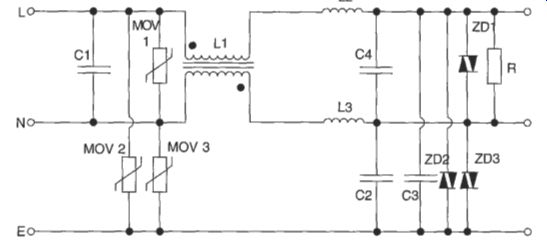
Fig. 14 Single-phase high-frequency power conditioner
Conducted emissions are attenuated by an electromagnetic interference (EMI) filter as shown in Fig. 13. The EM1 filter is a combination of LC filters for common-mode and differential-mode noise. In Fig. 13, C1 and C4 are X capacitors, which act with L2 and L3 to filter the differential-mode noise which flows between line and neutral connections. C2 and C3 are Y capacitors, which act with L1, L2 and L3 to filter the common-mode noise which flows through the earth connection and splits equally between line and neutral circuits. X capacitors have typical values in the range IO nF to 2 pF: these are used in cases where failure of the capacitor would not lead to a risk of electric shock. Y capacitors have typical values in the range 0.5 nF to 35 nF. These are used where failure of the capacitor could lead to risk of electric shock. The mutual inductance of L1 typically ranges from 1.8 mH at 25 A to 47 mH at 0.3 A, and L2 and L3 may be provided by the leakage inductance of the windings of L1. The resistance R is required in order to discharge the X capacitors with a time constant of typically 1 second.
Power conditioners limit the disturbances which enter a load from the ac supply.
They attenuate the high-frequency components of these disturbances using filters and by clipping voltage spikes. A typical single-phase power conditioner circuit is shown in Fig. 14. This circuit is similar to the filter circuit already shown in Fig. 13. but it has non-linear voltage clamping components added; these are shown as the metal oxide varistors MOV1, MOV2 and MOV3 and suppressor diodes ZDI, ZD2 and ZD3.
Radiated emissions may be suppressed by various forms of screens, including earthed enclosures, screens between transformer windings, screens between components and their heat sinks, and screens around the joints between the halves of ferrite cores.
The origin of high-frequency noise in switching power converters is the high rate of change of voltage and current during switching transitions. These high-frequency components in the waveform can be limited by minimizing the areas of the high- frequency current loops, and by using slow switching and snubbers. Components experiencing high rates of change of voltage propagate noise through capacitive coupling, and current loops with high rates of change of current propagate noise through radiated emissions.
The limits on Radio Frequency Interference (RFI) are usually required by law. This matter is dealt with in more depth in Section 15.
10. Systems with cascaded converters
The basic power conversion circuits which have been described are often combined in more complex applications. Some of the more common combinations are described in this section, and the merits of the different possibilities for some applications are set out.
10.1 The Uninterruptible Power Supply (UPS)
The UPS is used to provide a continuous stable supply in the event of a utility supply failure, this failure being typically defined as the ac voltage falling below 85 percent of its nominal value. Typical applications are in medical and communication systems, in which the expense of a UPS is justified by the reduced chances of a system failure.
The UPS therefore incorporates a back-up power source, which is usually a battery.
A typical scheme is outlined in Fig. 15. Such equipment is usually designed to provide 10-15 minutes' supply at full load, although to minimize the battery size some systems for computer supplies deliver the full load for just long enough for the hardware to shut down automatically and to save data. Diesel generators are often used where it is required to supply full load for longer periods,
Fig. 15 Typical on-line UPS block diagram
Most UPS systems are either on-line or standby types.
An on-line UPS continuously rectifies the utility supply, charges the back-up battery as necessary and supplies power to the load by continuously inverting the dc.
If the rectifier or inverter fails, a bypass switch is used to connect the load directly to the supply. When the utility supply fails, the back-up battery delivers dc power to the inverter and the ac supply to the load is maintained.
In a standby UPS, under normal operation the load is supplied directly from the utility network and the back-up battery is trickle charged. When a failure in the utility supply occurs, a changeover switch connects the output of an inverter to the load, and the inverter draws power from the battery. Standby systems are normally cheaper than on-line systems.
The line-interactive UPS is an off-line type which includes a system that boosts the supply voltage during line voltage sags. The voltage may be boosted by use of a tap-changing transformer. This system reduces the number of occasions when battery power is used; this helps to maintain a full charge in the battery for the event of a full The inverter is the heart of a battery-powered UPS, and different types are used for different applications. The cheapest systems deliver a square wave, but these require severe derating of power when supplying such loads as switched-mode power supplies. Inverters delivering a sinusoidal output are generally used. The ac output of the inverter is stepped up to the required output voltage using a transformer.
loss of supply.
10.2 Regulated dc power supplies
There is a large demand for power supplies that convert the utility ac supply to an isolated low-voltage dc output. This is mainly due to the near-universal use of transistor circuits for control, communication and computing equipment, these transistor circuits being powered by low-voltage dc.
For applications that require an accurately controlled output voltage, a switched- mode power supply or a linear regulator is necessary in order to compensate for fluctuations in the ac input voltage and to limit the variation of output voltage with load current. Switched-mode power supplies become economical above a few tens of watts output, but below this level linear regulators are often preferred, especially in rectifier capacitor.
Low-noise, high-reliability applications. The dc output voltage is accurately controlled by comparing it with a voltage reference and by using negative feedback. The amplified voltage difference is used to control the regulator. This scheme requires an accurate voltage reference, which is usually temperature compensated, and an error amplifier; these are usually integrated with other components in an IC.
In a linear regulator a supply-frequency transformer is used at the input for isolation and to reduce the voltage level to that required by the load. The transformer output is rectified into a capacitor, and load current flows through the linear regulator to the output. A typical linear power supply scheme is shown in Fig. 16. These supplies require a large, heavy transformer and their efficiency is typically only 30-60 percent. A large proportion of the losses occur in the regulator transistor, and they are dissipated using a large heat sink.
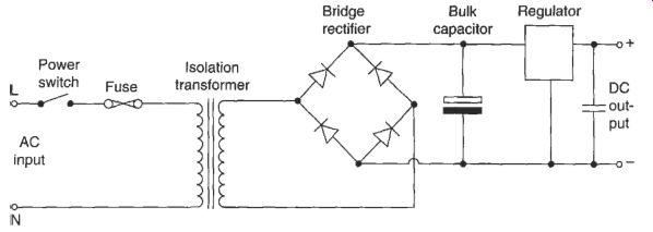
Fig. 16 Linear power supply scheme
Switched-mode power supplies use dc to dc converters. The ac supply is rectified into a capacitor, which results in some voltage ripple. The substantial dc power is passed through a dc to dc converter which regulates the output voltage using the switch duty cycle. The supply is isolated using a small high-frequency transformer.
This avoids the high power dissipation and the large transformer of the linear power supply, and efficiencies of 70-90 percent are usual. The circuit of a typical 1 kW to 10 kW off-line switched-mode power supply is shown in Fig. 17, and Fig. 18 shows a typical 100 W off-line power supply. A switched-mode power supply requires more components than a linear power supply; it also produces significantly more electrical noise because of the high-frequency switching, and this requires careful layout of the power circuit with filters and screens to limit the noise to acceptable levels.
Commercial dc power supplies may incorporate the following control and monitoring functions:
remote regulation of output voltage
shutdowns for thermal overload, transformer primary overcurrent and output overvoltage
external warning of power failure and external inhibit
output current foldback
parallel operation with forced current sharing
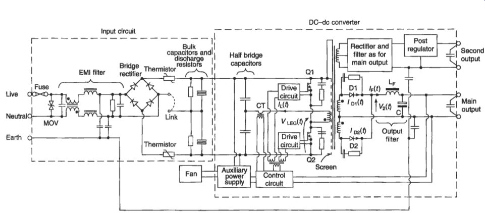
Fig. 17 A typical off-line switched-mode power supply power circuit
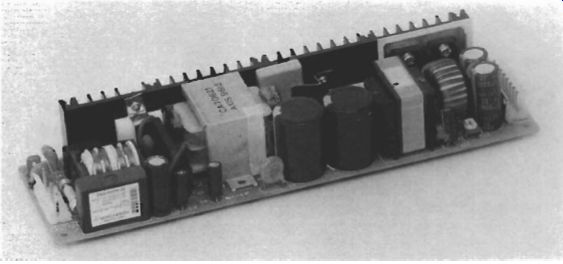
Fig. 18 A typical 100 W off-line power supply
10.3 Power conditioners for photovoltaic arrays
A typical photovoltaic array consists of relatively large-area silicon semiconductor diodes which are exposed to light that passes through a window. The diode is designed such that photons absorbed within the semiconductor often produce charge carriers in the form of electrons and holes. The increased carrier densities give rise to a voltage, and the ability to deliver electrical power. Many diodes are connected in series in order to provide sufficient voltage. A photovoltaic array delivers maximum power at a given voltage and current, but this optimum voltage and current varies with light intensity and temperature.
Photovoltaic cells may be used without power control circuitry to supply families of integrated circuits that have wide operating voltage ranges. However, most large systems use a peak power tracking converter which delivers the maximum power available at any instant, at a controlled dc voltage; this controlled power may be supplied to a static load, a battery or to an inverter.
Power converters which deliver ac output power to the utility network using a PWM inverter have been proposed for widespread use, but such systems are rarely practical at present because of the special requirements for connection of power generating equipment.
11. Standards
The leading international, regional and national standards adopted by users and suppliers of power supplies for manufacturing and testing are shown in Table 1.
Table 1 International, regional and national standards relating to power supplies
References
The first two references given below are academic treatments, and the third gives a design engineer's approach to low-power dc power supplies. Useful information can also be obtained from the catalogues of companies that distribute power supplies: these catalogues often include general technical information as well as information about specific products.
Mohan, N., Undeland T.M. and Robbins, W.P. Power Electronics: Converters, Appl. and Design, John Wiley & Sons Inc., 1995.
Williams, B.W. Power Electronics. Macmillan, 1992.
Billings, K.H. Switchmode Power Supply Hand book. McGraw-Hill, 1989.