AMAZON multi-meters discounts AMAZON oscilloscope discounts
1. Introduction
Power semiconductor switches are primarily used to control the flow of electrical energy between the energy source and the load, and to do so with great precision, with extremely fast control times, and with low dissipated power. The application of IC technologies on state-of-the-art power semiconductor devices has resulted in advanced components with low power dissipation, simple drive characteristics, good control dynamics, and switching power extending into the megawatt range.
Power semiconductor devices and control ICs are the key elements of power electronic systems-despite the fact that their costs are minimal in many applications, relative to the overall system costs. Improving their characteristics along with an increasing functionality reduces the system cost and opens opportunities for new fields of applications. New system trends are moving toward high switching frequency, reducing or eliminating bulky ferrites and electrolytes, as well as soft switching topologies for higher efficiency and low harmonies In electrical energy transfer, electronic devices are generally required to operate in "switch mode ". This means they should have ideal switch-like characteristics: they appear like a short-circuit passing current with minimal voltage drop across it in the on state; in the other side, they block the flow of current by supporting full supply voltage across it appearing like an open circuit in the off state. They operate in a different mode from power amplifying devices, which allow power transfer according to a linear relationship with an input signal, such as audio amplification. In switch mode operation, an electronic control signal is applied to turn the switch ON, and removed to turn the device OFF. For present devices, the control signal is typically in the 5-12 V range while the power supply voltage can be in the 20 V-8 kV range Solid state switch mode devices have been used for controlling power transfer for over 50 years.
Demands for the rational use of energy, miniaturization of electronic systems, and electronic power management systems have been the driving force behind the revolutionary development of power semi conductor devices over the last five decades.
As shown in FIG. 1, the power semiconductor switches cover all applications in the power range from 1W needed for charging the battery of a mobile phone, up to the GW range needed for energy trans mission lines (HVDC lines). As pointed out in this diagram, the bipolar devices (e g , thyristor, integrated gate-commutated thyristor [IGCT]) are a key technology for ultrahigh power systems while the MOS controlled devices (e g , insulated gate bipolar transistor [ IGBT], power MOSFET including SMART power systems) are the driving components for medium and low power electronic conversion systems. In the top power end, the switching frequency is below several 100 Hz, the medium power is dominated in the range of 10 kHz, but the system development for lower power is driven by several 100 kHz.
Advances in power electronic systems over the last three to four decades have been marked by five major inventions. Light-triggered thyristors and IGCTs in the top-end power range, IGBTs in the mid-and high-end power range, power MOSFET in the low-end power range, and SMART power systems for monolithic system integration, are mainly applied in automotive power. The bipolar transistor and the gate turn-off (GTO) thyristor don’t play a significant role in present development. For this reason, these device types are not focused on in this section.
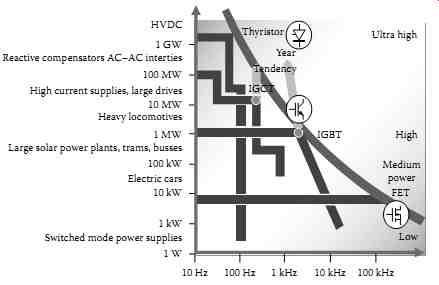
FIG. 1 Key fields of application versions switching frequency for power
semiconductor devices.
2. Brief History and Basics of Key Power Semiconductor Devices
2.1 Bipolar Device: thyristor
The first device developed 40 years ago, with many significant development steps, was the Si thyristor, a four-layer p-n-p-n structure allowing for very low resistance when turned on, and the ability to block voltage of up to 10 kV in the off state. It has a positive feedback mechanism for the buildup of current, once one of the p-n junctions in the structure is turned on. This is usually achieved by injecting a control current. The major drawback with the thyristor is that it cannot be turned off by applying a control signal. The same positive feedback mechanism that governs the current flow in a thyristor can only be stopped through "natural commutation," that is, when the conditions in the circuit to which the. thyristor is connected lead to current reversal through the device. Controlled turn-off mechanisms based on current transfer to ancillary circuits for short periods have been developed for thyristors. However, they were unsuited for rapid ON/OFF switch mode operations. Nevertheless, they were widely used in low-frequency switching applications due to their excellent on-state characteristics. They remain in use as rectifiers and inverters used in HVDC power transmission and as solid state control elements in static VAR compensators used for power factor optimization in the power network. The required voltage rating, up to 1000 kV for HVDC transmission systems, is obtained through serial connection of individual devices rated at 8-10 kV. Similarly, the current rating is obtained by parallel connection of device stacks, with each device typically rated for up to 6 kA.
2.2 Unipolar Device: Power MOSFET
A kind of revolution in switch mode control of power transfer was brought about by the advent of fully voltage controllable solid state devices capable of sustaining high off-scale voltages in the mid-1970s. This was the power MOSFET Current flow is vertical from drain, through an inversion channel placed on the top surface at right angles to the main current flow path, and into the source. The ability to control the current flow by application of a gate voltage to turn the device on and removal of the gate voltage to turn the device OFF are its main control features. This control principle of applying a gate voltage to a metal-oxide semiconductor (MOS) structure to create a conducting channel was, of course, well established for the low voltage MOSFET, and reliable gate fabrication technology was developed for integrated circuits by the mid-1970s. The advance of the power MOSFET was the double-diffused channel structure, with the channel being created in a diffused-body region rather than in the substrate, which allowed the device to have a p-n junction blocking region to support a large voltage in the off state. A power switch, however, with high current conduction in the on state is required.
In the power MOSFET, this was achieved by replicating millions of cells like those shown in FIG. 2.
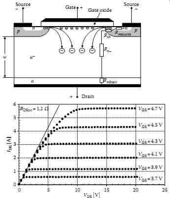
FIG. 2 Cell structure and I-V characteristics of a power MOSFET
Since the power MOSFET is a unipolar device and its current is carried only by charge carriers of one polarity (electrons for an n-channel device and holes for a p-channel device), it can be switched very fast (like resistors). This makes the power MOSFET ideally suited for high frequency switching.
Its major limitation, however, also arises from the unipolar nature of current flow, especially for high length of the lowly doped drift region, that also has to be increased together with a reduction in the doping concentration. Both these changes in design parameters tend to increase the on-state resistance of a power MOSFET switch according to the relationship R V on ~ max 2 5. However, if the on-state voltage is high, the static loss in the switch will be unacceptable. Because of this reason, the DMOSFET device shown in FIG. 2 is not practical for use as a power switch at voltage ratings in excess of 800. It can, however, be switched at frequencies as high as 5 MHz.
2.3 MOS-Controlled Bipolar Mode Power Device IGBT
The insulated gate bipolar transistor ( IGBT) has a MOS gate control structure identical to that of a power MOSFET. The only difference is that the n+ drain contact of the power MOSFET is replaced by a p+ minority carrier injector in the IGBT ( FIG. 3).
 FIG. 3 Cell structure and I-V characteristics of IGBT
Using this simple and elegant adaptation, a whole new class of hybrid MOS-bipolar solid state devices, being particularly aimed at power switching was demonstrated in the early 1980s. When the MOS channel is turned on, the p-n diode at the high-voltage terminal (anode) is turned on, and minority carriers (holes) are injected into the n-drift region. This is the classical conductivity modulation effect that can be achieved in a semiconductor by having charge carriers of two polarities carrying the current flow.
Hence the on-state resistance in the IGBT drift region is much lower than that in a MOSFET. In principle, the IGBT has all the advantages afforded by voltage control, inherent in a MOSFET, together with the low on-state voltage enabled by bipolar conduction. However, the large stored charge in the n-drift also severely reduces its high frequency and hard switching capability.
Over the last two decades, major efforts have been directed at optimizing the trade-off between low on-resistance and high turn-off losses in the IGBT. There efforts have led to the point where the IGBT is the device of choice for all power control applications at voltages from 600 up to 6500 V.
2.4 Key Power Device Development and their Major Characteristics
Originating from these basic structures, huge development steps have advanced the power semiconductor switches to the enabling technology for all energy efficiency power electronic system developments. Based on these principles, many new device families have become available , for example, light-triggered thyristor (LTT), power diodes, non-punch-through IGBTs (NPT- IGBTs), super junction power MOSFET (SJ-MOSFET), SiC devices (silicon carbide-based devices), and SMART power systems. In the following sections, these device concepts will be shown and their characteristics will be discussed.
3. Bipolar Devices
3.1 thyristor and LTT
The thyristor is a four-layer p+-n-p-n+ device. Since three p-n junctions are connected in series, the thyristor is able to block a negative (reverse blocking mode) as well as a positive voltage (forward blocking mode) applied between the anode (p+-layer) and the cathode (n+-layer). For positive anode-to-cathode voltages, switching of voltages up to more than 10 kV and currents up to several kA is possible by feeding a short current pulse in the inner p-layer. Such a trigger current can be provided either by a third electrical gate terminal or by using a light pulse ( FIG. 4). In the latter case, the light impinging into the device creates electron-hole pairs that are separated in the space-charge region of the reverse-biased inner p-n junction. The hole current flowing toward the cathode layer is used to trigger the thyristor.
Utilization of light-triggered thyristors is of particular benefit in applications with thyristors connected in series, since optoelectronic coupling and galvanic isolation is an inherent feature of light-triggered thyristor systems.
In order to minimize the turn-on current that is required to trigger the thyristor, several auxiliary thyristors, the so-called amplifying gate structures, are usually connected between the central trigger area (gate terminal or light-sensitive area) and the main cathode area of the thyristor. FIG. 4 shows two and four of such amplifying gate (AG) structures for the electrically-triggered and the light triggered thyristor, respectively. The trigger sensitivity of each amplifying gate can be adjusted easily , for example, by the width of its n+-emitter and/or the sheet resistivity of the p-base below the same.
As a rule of thumb, the minimum trigger current of two successive amplifying gates differs by a factor between 3 and 10.

FIG. 4 Electrical-triggered (left) and light-triggered thyristor (right).
Typical forward blocking and on-state current-voltage characteristics of high-power thyristors are depicted in FIG. 5. The hysteresis in the on-state characteristic results from the fact that the current has to distribute across the extended main cathode area after turn-on. In the 5 in. thyristor considered here, the current distributes over the entire cathode area, not until the current exceeds approximately 3 kA. Current spreading during the turn-on process and the final on-state voltage VT can be controlled by several measures: For large-area thyristors, the outermost AG is typically designed in such a way that the main cathode area is triggered along a preferably extended section, resulting in an AG structure that is distributed over the thyristor area ( FIG. 6). In addition, current spreading is influenced by the emitter shorts and the charge-carrier lifetime in the thyristor. Emitter shorts are local resistive connections distributed over the main cathode area and provide a bypass of the emitter junctions. Such emitter shorts are necessary to reduce the dV/dt sensitivity of the main cathode. However, extended emitter shorts distributed with a high density over the active area reduce the current-spreading velocity and lead to higher on-state voltages. These trade-off relationships have to be carefully accounted for when designing the emitter shorts. The same is valid for decreasing the charge-carrier lifetime, improving the dV/dt capability, and reducing the circuit-commutated turn-off period tq (the minimum time delay that is necessary, after a thyristor having been switched off by forced commutation, before the thyristor can withstand a positively biased voltage pulse), so as to decrease the current-spreading velocity and increase the on-state voltage VT. The charge-carrier lifetime can be adjusted very accurately by creating recombination centers. This can be achieved either by diffusion of heavy metals such as gold or platinum, or by creating irradiation defects by means of electron or light-ion irradiation. Since gold-related trap centers usually cause high leakage currents, in particular at elevated operating temperatures, and the recombination rate of platinum-related trap centers decreases significantly under low-injection conditions, the most used technique recently to adjust the charge-carrier lifetime is based on irradiation induced defects.
Finding the optimum charge-carrier lifetime is also of particular importance for optimizing the turn-off behavior (FIG. 7). Reducing the reverse-recovery charge Qrr and, consequently, the turn-off losses E_off is essential, since a standard thyristor cannot be actively turned off by a control signal. Instead, turn-off is usually achieved by commutating the anode-to-cathode voltage. As soon as the thyristor has reached the applied reverse voltage, the remaining charge carriers can disappear only by recombination. Thus, to accelerate the turn-off process a short charge-carrier lifetime is advantageous. FIG. 8 illustrates typical tq - VT and Qrr - VT trade-off relationships.
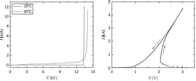
FIG. 5 Forward blocking current voltage characteristic of a 13 kV thyristor
(left). Typical on-state characteristic of a high-voltage thyristor (right).
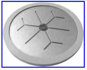
FIG. 6 Top view on a light-triggered thyristor, the line pattern in
the blank covering the main cathode area represents the shape of the
distributed outermost AG.
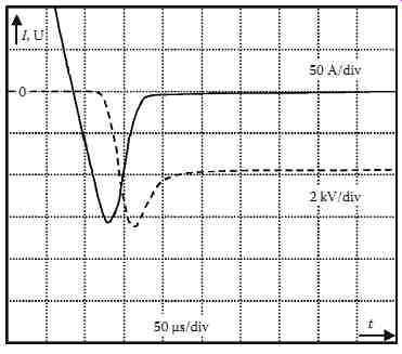
FIG. 7 Typical turn-off characteristics of a high-voltage thyristor
switched off by forced commutation.

FIG. 8 Schematic tq - VT trade-off relationship (left) and Qrr - VT
trade-off relationship (right) of a high-voltage thyristor.
Thyristors with high blocking voltages can be used not only for high-voltage direct-current (HVDC) transmission applications requiring a total blocking voltage capability up to 1 MV, but also in miscellaneous pulse-power applications, such as accelerators, cable analysis systems, crowbar applications (e g , klystron protection), discharge of capacitive and inductive storages (e g , series-capacitors protection), electromagnetic forming, spare of ignitrons, sterilization of foods and medical instruments, or switch gears. Today's commercial thyristors have maximum current ratings up to several kiloamperes, surge current capabilities of a few tens of kiloamperes, blocking voltage capability higher than 8 kV, and device areas up to 6 in. For many applications, thyristors require protection against a variety of failure modes. For example, the thyristor must be protected against destruction caused by overvoltage pulses or voltages with a voltage rise rate exceeding the maximum rated rise rate. In addition , for HVDC transmission applications, it’s necessary to avoid premature device turn-on when a forward voltage pulse is applied during the circuit-commutated turn-off period, because a thyristor is not able to withstand a forward voltage pulse with the rated blocking voltage or the rated maximum dV/dt value until the charge-carrier plasma is completely removed from the n-base. Such protection requirements can be achieved by the implementation of extensive monitoring and electrical protection circuitry.
However, recent developments in thyristor switches are aimed at reducing external electrical protection circuits by integrating the corresponding protection functions directly into the thyristor pellet as given in the following:
• Integration of an overvoltage protection function can be achieved by implementing a break over diode (BOD) in the light-sensitive area of a light-triggered thyristor ( FIG. 4). The voltage level VBOD, at which the overvoltage protection function is activated, can be adjusted by the distance between the central p region with radius rBOD and the concentric p ring with an inner radius rp. For large distances, the breakdown voltage is essentially determined by the curvature of the central p region. A reduction of the distance results in a reduction of the electric-field strength at the center of the BOD for a given voltage. For sufficiently small distances, the breakdown voltage approaches the value of the uniform p-n- junction;
• By designing the innermost AG such that its dV/dt sensitivity is higher than that of the other AGs and the main cathode, a safe turn-on of the device starting from the innermost AG is ensured, when the voltage rises at a rate higher than the threshold dV/dt rate of the innermost AG. By this means, a dV/dt protection function is integrated into the device in addition to the overvoltage protection function. Apart from the geometrical dimensions of the AGs, the sheet resistivity of the p-base is an important parameter to adjust the dV/dt sensitivity of the AGs;
• In order to protect the thyristor from being destroyed during the circuit-commuted turn-off period, the thyristor should be turned on in a controlled way by the AG region when the thyristor is loaded by a forward voltage pulse during the circuit-commutated turn-off time. However, since the AGs usually turn off earlier than the main cathode area, there are typically fewer free charge carriers below the AG structure compared to the main cathode area. Two measures can be used to overcome this problem: First, the radial distribution of the charge-carrier lifetime should be modified such that it’s reduced in the main cathode area of the device compared to the AG region. Secondly, phosphorus islands implemented into the p-emitter in the inner AG structure ( FIG. 4, right) form the emitter of local n-p-n transistors when a reverse voltage is applied to the device and therefore provide further support for re-triggering in the AG region when a for ward voltage pulse is applied to the device. The carrier injection of these islands can be controlled by their sizes and their doping profile.
Integrating these three protection functions provides a completely self-protected, directly light triggered thyristor, ensuring a reliable operation with a drastically reduced monitoring and protection circuitry.
3.2 Gate turn-Off thyristor and Integrated Gate-Commutated thyristor
3.2.1 the GTO thyristor
A gate turn-off (GTO) thyristor is a special type of thyristor. GTO thyristors, as opposed to normal thyristors, are fully controllable switches that can be turned on and off by their third lead, the gate lead.
Thyristors can only be turned off by reducing the on-state current below the holding current. Therefore, thyristors are not suitable for applications with DC power sources. The GTO thyristor can be turned on by a gate signal, and can also be turned off by a gate signal of negative polarity Turn-on is accomplished by a positive voltage pulse between the gate and cathode terminals. The typical gate voltage is in the range of 15 V. The turn-on phenomenon in GTO thyristors is, however, not as reliable as in a thyristor and a small positive gate current must be maintained even after turn-on to improve reliability. Amplifying gate structures, which are very helpful for the turn-on of the thyristor, are not implemented in GTO thyristors.
Turn-off is induced by a negative voltage pulse between the gate and cathode terminals. Some of the forward current (about one-third to one-fifth) is used to induce a cathode-gate voltage, which in turn results in a decrease of the forward current, and the GTO thyristor will switch off. Usually, the carrier lifetime in the base region has to be reduced by a well-defined creation of recombination centers to shorten the tail phase and to keep the turn-off losses low. These recombination centers can be generated by electron or helium irradiation, resulting in crystal defects effecting deep levels in the band gap.
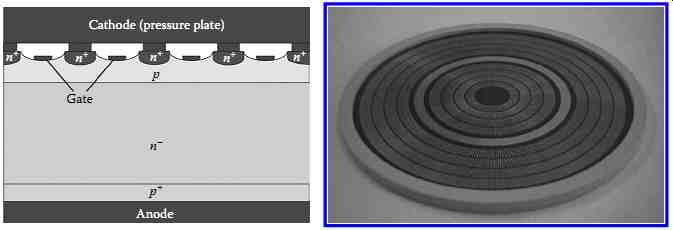
FIG. 9 Cross-section (left) and top view of a GTO thyristor with mesa
cathode structure (right)
The cross section and the top view of a GTO thyristor are illustrated in FIG. 9. There are many small emitter mesa structures distributed along the device, which are identical in width and length, to guarantee a relatively homogeneous flow of the turn-off current. The homogeneity of the current flow during the turn-off period is a very critical point because such inhomogeneities result in current filamentation and with it in dynamic avalanche. The resulting local self-heating effects can be so strong that the device burns out. Therefore, the maximum current, which can be turned off without destroying the device, can be significantly reduced by inhomogeneities of the turn-off current induced , for example, by an inhomogeneous distribution of the carrier lifetime in the n-base, of the p-base resistance, of the penetration depth of the n-emitter/p-base junction, or of the contact resistance between metallization and semiconductor. Also, mechanical stress effects can play an important role. Therefore, it’s extremely important to guarantee clean processing and homogeneous doping processes.
To keep the electrical field strength induced by dynamic avalanche as low as possible, the transistor gain a pnp has to be chosen very carefully. For that purpose, the hole injection by the p-emitter has to be limited , for example, by a vertically inhomogeneous carrier lifetime reduction with a high recombination rate below the p-emitter or by a limitation of the emitter efficiency by a relatively small doping concentration of the p-emitter GTO thyristors suffer from long switch-off times, whereby after the forward current falls, there is a long tail time where residual current continues to flow until all remaining charge from the device is taken away. This long current tail restricts the maximum switching frequency to approximately 1 kHz.
It may be noted, however, that the turn-off time of comparable symmetrical controlled rectifiers (SCRs) is about 10 times that of a GTO thyristor. Thus, switching frequency of GTO thyristors is much better than that of SCRs. The main applications of such GTO thyristors are in variable speed motor drives, high-power inverters, and traction GTO thyristors are available either with or without reverse blocking capability. Reverse blocking capability enhances the forward voltage drop and the dynamic losses because of the need to have a thick, low doped base region. GTO thyristors capable of blocking reverse voltage are known as sym metrical GTO thyristors. Usually, the reverse blocking voltage rating and forward blocking voltage rating are about the same. The typical application for symmetrical GTO thyristors is in current source inverters.
GTO thyristors incapable of blocking reverse voltage are known as asymmetrical GTO thyristors. They typically have a reverse breakdown rating in tens of volts or less. By the use of the anode shorts, the forward blocking capability of the device is enhanced due to the reduced transistor current gain a pnp, especially for high temperature operation. Asymmetrical GTO thyristors are used, where either a reverse conducting diode is applied in parallel ( For example, in voltage source inverters), or where reverse voltage would never occur ( For example, in switching power supplies or DC traction choppers).
Asymmetrical GTO thyristors can be fabricated with a reverse-conducting diode in the same package. These are known as reverse conducting (RC) GTO thyristors.
Unlike the IGBT, the GTO thyristor requires external devices to shape the turn-on and turn-off cur rents to prevent device destruction. During turn-on, the device has a maximum dI/dt rating limiting the rise of current. This is to allow the entire bulk of the device to reach turn-on before full current is reached. If this rating is exceeded, the area of the device nearest the gate contacts will overheat and melt from overcurrent. The rate of dI/dt is usually controlled by adding a saturable reactor. Reset of the saturable reactor usually places a minimum off-time requirement on GTO thyristor-based circuits. During turn-off, the forward voltage of the device must be limited until the current becomes small. The limit is usually around 20% of the forward blocking voltage rating. If the voltage rises too fast during turn-off, not all of the device will turn off, and current filamentation occurs so that the GTO thyristor will be destroyed due to self-heating effects induced by the high voltage and current focused on a small portion of the device. Substantial snubber circuits have to be added around the device to limit the rise of voltage at turn-off. Resetting the snubber circuit usually places a minimum on-time requirement on GTO thyristor based circuits.
The minimum on and off time is handled in DC motor chopper circuits by using a variable switching frequency at the lowest and highest duty cycle. This is observable in traction applications, where the frequency will ramp up as the motor starts, then the frequency stays constant over most of the speed ranges, and finally the frequency drops back down to zero at full speed.
3.2.2 the IGCT
The integrated gate-commutated thyristor (IGCT) is a special type of GTO thyristor and, like the GTO thyristor, a fully controllable power switch. It can be turned on and off by a gate signal, has lower conduction losses as compared to GTO thyristors, and withstands higher rates of voltage rise (dV/dt), such that no snubber circuits are required for most applications. The main applications are in variable frequency inverters, drives, and traction.
The structure of an IGCT is very similar to a GTO thyristor. In an IGCT, the gate turn-off current is greater than the anode current. This results in shorter turn-off times. The main difference compared with a GTO thyristor is a reduction in cell size, combined with a much more substantial gate connection, resulting in a much lower inductance in the gate drive circuit and drive circuit connection. The very high gate currents and the fast dI/dt rise of the gate current means that regular wires cannot be used to connect the gate drive to the IGCT. The drive circuit printed circuit board (PCB) is integrated into the package of the device. The drive circuit surrounds the device and a large circular conductor attaching to the edge of the IGCT die is used. The large contact area and short distance reduces both the inductance and resistance of the connection. The IGCT's much shorter turn-off times compared with GTO thyristors allows it to operate at higher frequencies. Up to several kilohertz for very short periods of time are possible. However, because of high switching losses, typical operating frequencies are up to 500 Hz.
IGCTs are also available either with or without reverse blocking capability. IGCTs capable of blocking reverse voltage are known as symmetrical IGCTs. The typical application for symmetrical IGCTs is in current source inverters. IGCTs incapable of blocking reverse voltage are known as asymmetrical IGCTs. They typically have a reverse breakdown rating in tens of volts or less. Such IGCTs are used where either a reverse conducting diode is applied in parallel or where reverse voltage would never occur. Asymmetrical IGCT can be fabricated with a reverse-conducting diode in the same package.
These are known as reverse conducting (RC) IGCTs.
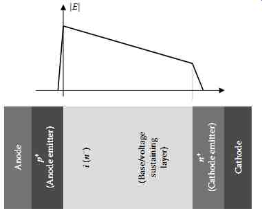
FIG. 10 Cross-section of a p-i-n diode and distribution of the electric
field in blocking operation.
3.3 Power Diodes
There are three major uses of power diodes in power electronic systems-line rectifiers, snubber diodes, and freewheeling diodes-which have different requirements on the electrical characteristics of the diode A line rectifier allows a current flow during one half wave of the applied sinusoidal voltage and has to block the current flow during the next (e g , negative) half wave of the voltage. The basic requirement is a low forward voltage drop that leads to low forward losses and the capability to carry large surge currents, which may occur especially during turning on of the system. On the other hand, these line rectifiers have to block the peak voltage of the line and some voltage peaks , for example, those caused by transients of other loads. The transition from forward to blocking operation is rather slow, depending on the line frequency (typically 50 or 60 Hz) and the peak voltage. The voltage slope is in the range of a few V µs-1 or below, even at high peak voltages in the range of a few kV. The requirements of high blocking voltage and high current capability for the same device are supported by a p-i-n-structure. Technically, these devices frequently use a slightly n-doped material as the example in FIG. 10 shows. The voltage-sustaining layer has a width and doping concentration adjusted to the required blocking capability. As a rule of thumb, the thickness of the voltage-sustaining layer is 10 µm per 100 V blocking voltage , for example 100 µm for a 1000 V device. The maximum doping concentration of the voltage-sustaining layer is below 10^17 cm^-3 , approximately, divided by the blocking voltage in V.
During forward operation, the voltage-sustaining layer is flooded by electrons and holes coming from the anode and cathode emitters and resulting in a charge plasma with a much higher carrier concentration compared to the background doping and thus in a lowered series resistance of the line rectifier. Line rectifiers require strong emitter structures at anode and cathode to build up much excess charge for low series resistance and low conduction losses of the device. Before the line rectifier can be turned from forward into blocking operation, the excess charge stored in the voltage-sustaining layer must be removed. Thus, high excess charge leads to high turn-off energy losses of the diode, but since the operating frequency is low, the total losses are still dominated by the conduction losses in forward operation.
The threshold of the p-n junction leads to the lower limit for the forward voltage drop. For Si-based diodes, the minimum is around 0.7 V. In contrast to line rectifiers, snubber diodes and freewheeling diodes are operated at higher frequencies (some 100 Hz up to 20 kHz) and with higher voltage slopes during commutation as the switching of the diode from forward to blocking operation is called. The turn-off losses of these diodes cannot be neglected, thus an optimum operating point must be found depending on the operating frequency.
Snubber diodes are used in the connection from a power switch (e g , GTO) to a capacitor of a snubber network, which reduces inductive peak voltages when turning off the power switch. A snubber diode should have a high current capability when turned on and low excess charge before a reverse voltage is applied to the diode.
To reduce the excess charge during static operation, recombination centers are introduced into the base of the diode. When reducing the carrier lifetime, the carrier concentration during the forward pulses is reduced. On the other hand, strong anode and cathode emitters lead to the required high surge current capability of the snubber diode. The forward current drops automatically when the peak voltage at the power switch ends, thus the turn-off behavior of a snubber diode is of minor importance.
In contrast to other diodes , for freewheeling diodes the turn-off characteristic is of high importance. The switching characteristic is dominated by the carrier distribution during forward operation of the chip and the doping profile in the voltage-sustaining layer. To reduce the switching losses, the electronic designer strives for decreasing the switching time of the diode. Freewheeling diodes are used , for example in converters in conjunction with GTO and IGBT switches.
Faster switching, however, leads to more critical conditions for a hard cut off of the reverse cur rent, which is not desired. Second, the stress on the diode during commutation is critical. At the time when the high reverse current is extracting the excess charge of the diode, already considerable reverse voltage lies at the diode terminals. Of course, the stress must not exceed the capability of the freewheeling diode. Softer switching and higher robustness at commutation are the enablers for reduced dynamic losses of the diode. In recent years, considerable softer switching of freewheeling diodes was achieved.
Also, the understanding of the robustness led to significantly improved robustness also in the area of higher blocking voltages up to 6 5 kV For applications at even higher frequencies , for example in switched mode power supplies (SMPS) where diodes are commutated at frequencies up to 300 kHz, it can be technically and economically advantageous to use two diodes in series, with each half the required blocking capability since the turn-off losses of diodes grow approximately quadratic with their blocking voltage. As a drawback, two diodes connected in series exhibit twice the threshold voltage. At the high end of switching frequencies, Schottky diodes based on wide-gap semiconductors, which behave like a small capacitors when they are commutated, provide least losses and therefore least system cost despite their being more expensive compared to conventional silicon devices with the same static forward current and blocking capability.
4. MOS-Controlled Bipolar Mode Device
Similar to unipolar MOS-controlled devices, the blocking capability of MOS-controlled bipolar mode devices increases with the thickness of the region along the space-charge region developing when a blocking voltage is applied. However, while the charge-carrier concentration in the on state for unipolar devices is mainly determined by the doping concentration of this region, it can be increased toward much higher values in bipolar devices. Consequently, switching losses and the switching behavior can be optimized to a large extent independent from the doping concentration of the drift region in MOS-controlled bipolar devices. The most successful MOS-controlled bipolar switch is the IGBT, which is employed in miscellaneous applications in the voltage range from 300 V up to 6 5 kV.