AMAZON multi-meters discounts AMAZON oscilloscope discounts
(<< cont. from prev.)
4.1 IGBT
4 1.1 Basic Concepts
FIG. 11 shows three vertical IGBT designs with the aid of a planar DMOS cell. Similar to the MOSFET, the blocking voltage is sustained by the p-n junction formed by the p-body and the weakly doped n-base. The distinctive difference between the MOSFET and the IGBT is that the n-doped drain is replaced by a p-doped backside collector that is able to inject holes into the n-base. When the gate voltage exceeds the threshold voltage, the n-base will be flooded by electrons injected from the n-doped source layer through the n-channel and by holes from the p-doped backside layer. As a consequence, a charge-carrier plasma evolves in the n-base. The charge-carrier concentration in this plasma (>10^16 cm^-3 ) is typically several orders of magnitude higher than that of the doping concentration (<10^14 cm^-3 ) of the weakly doped n-base. Thus, despite the low doping concentration of the n-base that is required to sustain high blocking voltages in the off state, the voltage drop in the on-state voltage of the IGBT for a given current can be kept much lower than that of a MOSFET with the same blocking voltage capability due to the conductivity modulation in the n-base.
Each of the three IGBTs structures shown in FIG. 11 has specific advantages: the non-punch-through (NPT) IGBT is characterized by the thick weakly n-doped drift region. Its width is chosen so long that the electric-field strength drops to very small values inside this drift region under any opera ting condition--even when the maximum rated voltage is applied between the emitter and collector contact. The desired trade-off between the saturation voltage and the turn-off losses can be adjusted easily by the implantation fluence of the backside emitter, without the need of an additional charge-carrier lifetime reduction.
Moreover, the switching losses of an NPT IGBT depend only weakly on the operating temperature. The drift region in the punch-through (PT) IGBT is much shorter compared to an NPT IGBT, resulting in a lower on-state voltage. To ensure the same blocking capability of the PT IGBT, however, an additional n-doped buffer layer between the drift region and the thick p-substrate is required. A major disadvantage of the PT IGBT concerns the alignment of the backside emitter efficiency by means of the buffer layer or an additional charge-carrier lifetime reduction.
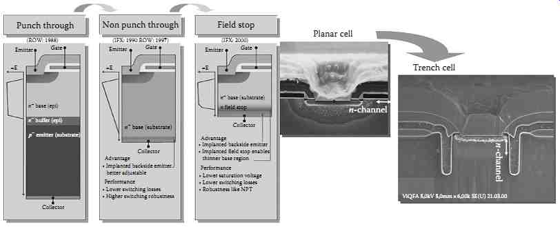
FIG. 11 Evolution of the vertical structure (left) and the cell structure
(right) in IGBT development.
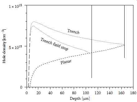
FIG. 12 Vertical cross-sections of the hole distribution from the emitter
to the cathode contact in IGBTs with different cell structures. The backside
emitter is located at a depth of 165 µm for the trench and the planar
cell and at about 110 µm for the trench field stop design.
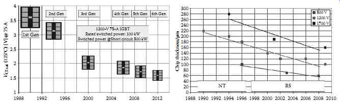
FIG. 13 Evolution of the chip area and VCEsat (left) and chip thickness
(right) in IGBT development.
The field-stop concept, or similar approaches like light-punch-through, soft-punch through, or controlled-punch-through [20], combines the advantages of NPT and PT IGBTs. The design parameters of the field-stop layer mainly determine the blocking voltage capability and the turn off behavior. A major challenge was, and still is, the handling of large-area and thin wafers to make the independent adjustment of the backside emitter efficiency by standard implantation processes possible.
In recent years, sophisticated technology processes have been developed so that , for example, 600 V IGBTs with a thickness well below 70 µm can be fabricated from 8 in. wafers.
Another important step to reduce on-state and switching losses was achieved by modifying the cell structure and the development of the trench cell. The horizontal position of the n-channel along the front side changes to vertical position and provides potential for chip-area shrinking due to the transition from the planar design to the trench structure. However, just as important is the effect of the trench structure on the vertical charge-carrier distribution between the cathode and the anode contact. The trench acts as a kind of bottleneck for the holes flowing from the backside anode contact toward the cathode, resulting in a drastic increase of the concentration near the cathode. For a properly designed trench structure, the increase in the hole concentration near the trench region can become so large that the hole concentration along the entire drift region exceeds that of a comparable planar cell. Because of charge neutrality, the electron distribution changes similarly. Since approximately three-fourths of the total load current is carried by the electron current, the on-state losses can be significantly reduced in the trench cell with relatively little influence on the switching losses, resulting in an improved Eoff -VCEsat trade-off relationship compared to the planar cell structure.
Thus, both decreasing the chip thickness and improving the cell design are key factors to reduce the active chip area. The evolution of the chip thickness and the chip area of IGBTs during the last years are illustrated in FIG. 13. Another important aspect for improving the Eoff –VCEsat trade-off relationship concerns the cell density. Since the electron current through the channel acts as a base drive for the p-n-p transistor of the IGBT, decreasing the channel resistance results in a stronger hole injection from the anode and, consequently, in lower on-state voltages. As the channel resistance decreases with the channel width, the increase in the cell density results in a significant improvement of the Eoff –VCEsat trade-off relationship ( FIG. 14). Typical output characteristic of a 75 A 1200 V IGBT are shown in FIG. 15.
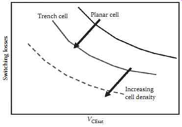
FIG. 14 Schematic Eoff –VCEsat trade-off relationship: Comparison of different cell designs and influence of the cell density.
The turn-off behavior of a trench field-stop IGBT is shown in FIG. 16. At the beginning of the turn-off period, the IGBT is in the conductive state, since the gate-emitter voltage is significantly higher than the threshold voltage. Consequently, the collector-emitter voltage drop is very low (<2 V). The collector current is limited by the load. Once the gate potential VGE changes from 15 V to −15 V, a gate current rises to discharge the input capacitance that is essentially formed by the parallel connection of the gate-emitter and the gate-collector capacitance. The approximately exponential decay of the gate-emitter voltage continues until the threshold voltage is reached. Due to the inductive load, the collector current cannot drop immediately, but is maintained by the extraction of charge carriers. In this initial phase of the turn-off period, the turn-off characteristics of the IGBT are similar to that of a MOSFET. Before the current can start dropping, the collector-emitter voltage must rise. Once the threshold voltage is reached, the gate-emitter voltage is initially constant (Miller plateau), since nearly the entire gate current is needed to discharge the gate-collector capacitance.
As this capacitance decreases with increasing collector voltage, the gate current can start to discharge the gate-emitter capacitance again (end of the Miller plateau) so that the gate-emitter potential drops further. The ensuing voltage overshoot is caused by the voltage drop induced by the stray inductance in the load circuit due to the decreasing collector current. A distinct difference compared to the turn-off behavior of the MOSFET is the appearance of the so-called tail current at the end of the turn-off phase. This tail current is caused by excess carriers in the IGBT that don’t appear in the unipolar MOSFET.
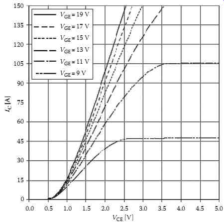
FIG. 15 Typical output characteristic of a 75 A 1200 V IGBT at 125°C.
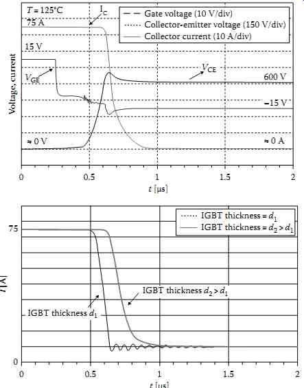
FIG. 16 Turn-off characteristics VGE(t), VCE(t), and IC(t) of a 75
A 1200 V IGBT at 125°C under nominal conditions (top) and turn-off current
IC(t) for two IGBTs with different device thickness and an additional
stray inductance of 400 nH at 25°C (bottom). The measurements were performed
with a module so that the measured gate signal represents not the gate
potential of the IGBT but is shifted by the potential drop across an
ohmic resistance inside the module.
The influence of the thickness on the turn-off behavior of an IGBT is also illustrated in FIG. 16.
Two IGBTs with different chip thicknesses were stressed with an additional stray inductance of 400 nH in the load circuit. The thinner IGBT has less stored excess carriers. Consequently, turn-off is faster compared with the thicker IGBT. However, at the end of the turn-off phase, the excess carrier density in the thinner IGBT is too low to support the load current, so that the current abruptly decreases, resulting in the excitation of voltage and current oscillations from the resonant LC resonant circuit that is formed by the stray inductance L and the capacitance C of the IGBT. The higher excess charge in the thicker IGBT, however, results in soft turn-off without any oscillations.
An important feature of the IGBT is its ability to withstand a short circuit for a certain time interval.
Today's IGBTs are typically able to resist a short circuit for a period of 10 μs. This period provides enough time to detect the fault and turn off the IGBT by an external monitoring circuit. The short-circuit current is usually considerably higher than the rated current. Thus, if the nominal voltage is applied to the device during the short-circuit period, there is a huge energy dissipation in the IGBT, resulting in a strong self heating of the device. If the device is not turned off fast enough, the current will increase in a way that is no longer controllable due to the activation of the parasitic thyristor formed by the source, the p-body, the n-drift region, and the p-emitter, so that the device will eventually be destroyed.
4.1.2 Advanced Concepts
4.1.2.1 Reverse Conducting IGBT
In an RC- IGBT, a diode is monolithically integrated into the IGBT chip. For volume production, this concept was first realized with an optimization for soft-switching applications such as lamp ballast or inductive heating applications in the 600 V and 1200 V class. Meanwhile, also RC- IGBTs for hard switching applications, such as industrial inverters or drive applications have been developed on the basis of the NPT-technology.
FIG. 17 shows the cross section of an RC- IGBT, based on a trench field-stop IGBT. The n-doped regions at the backside act as a cathode emitter, while the p-body of the IGBT and the highly p-doped anti latch-up region near the frontside act as an anode emitter of the integrated diode. Thus, the IGBT is able to conduct a current even when the polarity of the collector-emitter-voltage is reversely biased.
Major challenges for RC- IGBT production are, particularly for thin wafers, the necessity of a backside photolithographic process, and particularly for higher load currents, the robustness of the diode.
Moreover, integration of the diode and the IGBT into the same chip makes the independent adjustment of the charge-carrier distribution in the diode and the IGBT difficult. However, it has been shown that the Qrr-Vf trade-off relationship of the diode can be significantly improved by lifetime control techniques sustaining a good IGBT performance.
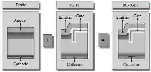
FIG. 17 Integration of a diode and an IGBT resulting in a reverse conducting
IGBT.
4.1.2.2 Carrier Stored Trench Bipolar Transistor IGBT
As illustrated above in the light of the trench IGBT, the on-state and switching losses can be optimized by tailoring the charge-carrier distribution in the IGBT. The increase in the hole concentration in the trench IGBT , for example, results in a drastic decrease of the on-state voltage. In the carrier stored trench bipolar transistor (CSTBT), this increase in the hole concentration is further strengthened by the implementation of an additional n-doped layer below the channel region ( FIG. 18). The n-doped layer forms a barrier for holes moving from the anode to the cathode, resulting in an increase in the carrier concentration. If the doping concentration is properly designed, the blocking capability of the IGBT won’t significantly be reduced.
A stripe-shaped trench design as indicated in the schematic of the CSTBT is typically characterized by a big gate capacity and a high short-circuit current. These disadvantages can be avoided by deactivating a part of the trenches. Such a trench deactivation can be easily achieved , for example, by connecting the respective trenches not to the gate contact but to the emitter contact ( FIG. 18).
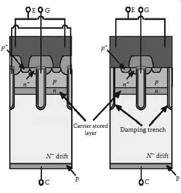
FIG. 18 CSTBT (left) and CSTBT with inactive trenches (right).
4.1.2.3 Clustered IGBT
In order not to deteriorate the blocking capability of a CSTBT, the maximum doping concentration of the n-doped layer, and consequently, the increase in the carrier concentration is limited. The clustered- IGBT (C IGBT) shifts this limitation to higher values of the doping concentration by the implementation of an additional p-well directly below the n-doped layer ( FIG. 19). The C IGBT can be built as planar or trench IGBT. The floating p-well is part of an internal thyristor formed by the p-anode, the n-drift, the p-well, and the n-well. In FIG. 19, the single gate contact of the C IGBT is divided into two parts in order to elucidate the function of the device: Turn-on of the C IGBT is essentially controlled by gate-2. If the gate voltage surpasses the threshold voltage, the n-drift and n-well region are connected to source potential and the potential of the floating p-well rises with increasing positive anode voltage. Once the p-well potential exceeds the built-in voltage of the p-n junction formed by the p-well and the n-well, the internal thyristor turns on without snap-back. In this operation mode, the load current of the C IGBT is controlled by the potential of gate-1. If the anode voltage is increased under this condition, the main part of voltage drops across the p-n junction formed by the p-base and the n-well. Turn-off of the C IGBT is achieved by reducing the gate voltage to zero so that the electron current feeding the internal thyristor is interrupted.
IGBTs with dynamic clamping capability for overvoltage self-protection.
Recently, much work has been done to provide the IGBT with a so-called dynamic clamping capability that enables the device to regulate its voltage during turn-off to a level that is close to the rated voltage.
The integration of such a dynamic overvoltage self-protection function renders superfluous external control and protection circuits for voltage clamping and gives the user more freedom concerning the selection of the optimum gate resistance for his application. However, ensuring that dynamic clamping works properly under all possible operating conditions is a challenging task. Important design parameters that can be used to enhance the dynamic clamping capability of a field-stop IGBT are the doping dose of the field-stop layer and the backside p-emitter. Both lowering the field-stop layer dose and increasing the backside p-emitter dose result in a better dynamic clamping capability. However, these doses cannot be adjusted arbitrarily without deteriorating other characteristics of the device. Reduction of the field-stop dose , for example, is limited by the required breakdown voltage. A higher backside emitter dose is in particular critical for fast-switching IGBTs, because more charge carriers have to be removed during the turn-off period.
Furthermore, shifting of the initial breakdown from the junction termination into the trench-cell area by appropriate cell and junction termination design is important to avoid destruction in the cell area close to the junction termination area. One possibility to achieve this shifting is to use different trench geometries for the trenches near the junction termination and that in the cell area. Another possibility is to lower the breakdown voltage in the cell area by increasing the doping concentration of the n-doped drift region locally, near the p-n junction formed by the p-body and the n-drift region. It’s also possible to expose the junction termination area to light-ion irradiation, to shift the breakdown voltage of the junction termination area and its nearby trench cells to higher values.
As an example, FIG. 20 illustrates the successful dynamic clamping for a turn-off current of twice the rated current of a 1200 A module with 16 parallel-connected 75 A 1200 V trench IGBT chips that are stressed by a 400 nH stray inductance. Even under this hard condition, the integrated dynamic clamping function operates reliably and the clamping voltage does not significantly exceed the rated voltage.
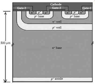
FIG. 19 3.3 kV planar C IGBT.
Meanwhile, several investigations on IGBTs with dynamic clamping capability have been reported for voltage classes ranging from 1.2 up to 6.5 kV (e.g., [30-33]). It’s worth noting that a C IGBT can also be provided with a self-clamping function: if the p-n junction formed by the p-base and the n-well region is properly designed, punch-through at a certain anode voltage results in a voltage clamp.
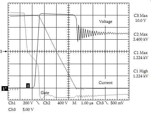
FIG. 20 Overcurrent (twice the rated current) turn-off behavior of
a 1200 A 1200 V module with a DC link voltage of 900 V, an estimated
worst-case stray inductance of 400 nH at an ambient temperature of 125°C.
5. Unipolar Devices
5.1 High-Voltage Power MOSFET
In certain applications, minimizing the volume, weight, and of course the cost of transformers and other inductive devices is aimed at, which is done by increasing the operation or switching frequency of power devices. SMPS, as used in many consumer or information technology appliances, are one example for these applications. Here, switching frequencies between 30 and 300 kHz are common today with a blocking capability of the switches between 200 and 1000 V. Operation of IGBTs , for example, at these frequencies is possible, but result in rather high dynamic losses. Power MOSFETs have higher on state resistance compared to IGBTs with the same chip area, but they also have no charge plasma resulting in much lower turn-off losses. On the other hand, the on-state resistance per chip area increases with the blocking capability as sketched in FIG. 21.
The reason behind this is that higher blocking voltages require thicker voltage-sustaining layers with lower doping. Since the load current flows directly through this voltage-sustaining layer, it forms a series resistance that-at least for high-voltage power MOSFETs above 200 V-dominates by far the overall resistance of the device.
Selecting a 500 V MOSFET , for example, with low on-state resistance for a given application, would result in a device with a correspondingly large and expensive chip area. A large chip area exhibits large stray capacities, which have to be charged and discharged during each turn-on and turn-off of the device, resulting in comparative slow switching transients. These slow switching transients help to reduce electromagnetic interference (EMI) and ringing, mainly in disadvantageous layouts. But on the other hand, slow switching transients waste switching energy and, due to the rather high switching frequency, impair the efficiency of a design. Worse efficiency directly leads to oversize the power switches and heatsinks to solve thermal issues.
A professional system designer will strive for an EMI conform layout and using fast-switching devices to get an efficient and compact solution for the application at least cost.
The major tasks for the device manufacturer are to provide high-voltage power transistors with less switching losses, ergo smaller parasitic capacitances and lower on-state resistance per chip area. Both tasks can be accomplished by reducing the area-specific on-state resistance, since smaller chips with the same nominal on-state resistance also have smaller parasitic capacitances.
Practically a higher doping of the voltage-sustaining layer will lead to more carriers available for current transport. On the other hand, such a device would lead to a lower blocking voltage capability. The way out of this dilemma was the introduction of a doping of the opposite type close to the doping of the current bearing path [34,35] to have local high conductivity and global low doping due to the compensation.
It took several years until the first devices were commercially available that successfully used this approach. Since then, the doping compensation devices were the development path for improved high-voltage MOSFETs using different manufacturing approaches and optimization goals.
Beyond all these developments lies the same basic structure as in the right part of FIG. 22, which is compared to a conventional power MOSFET (left part). Both devices basically have the same structures on the chip front side with a gate controlling an inversion channel.
Here, the voltage-sustaining layer consists of donor (n−) and acceptor (p−) doping situated in two individual regions. For blocking operation, the difference of donor and acceptor doping determines the blocking voltage. This net doping is comparable to the very low doping of the voltage-sustaining layer for a conventional power MOSFET. The donor doping of the most modern devices can be increased by a factor of 15 or more compared to standard MOSFETs and thus the on-state resistance is reduced by a factor of 7.5 or more.
Since the blocking characteristic is determined by the difference of a comparatively high donor and acceptor doping the control of this net doping becomes the most challenging task.
When building up a blocking voltage at closed channel, a space-charge region starts extending from the folded pn-junction into the p compensation columns and into the n current path. The width of this insulating region grows with rising blocking voltage as sketched in FIG. 23. Already, at rather low blocking voltages applied between drain and source compared to the blocking capability, almost the whole area of current path and compensation column is depleted.
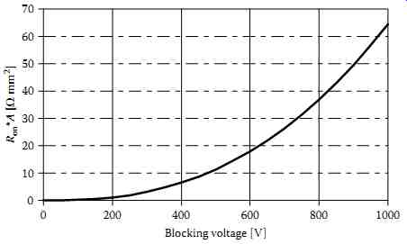
FIG. 21 Dependence of the series resistance of a MOSFET of the blocking
voltage. One major advantage is the reduction of the parasitic capacitances
of compensation devices, especially at higher drain-source voltages as
depicted in FIG. 24. This leads to lower control power needs and to much
faster switching, thus lower overall dynamic losses. The nonuniform curves
for the drain-source capacitance originates from the building up of the
insulating space-charge region with increasing blocking voltage between
drain and source as depicted in FIG. 23.
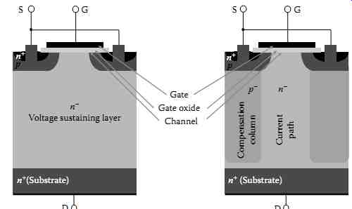
FIG. 22 Left: Cross section of a conventional vertical n-channel power
MOSFET: The load current is controlled by the gate and flows from the
n source on the front surface of the chip towards the drain on the rear
surface through the low doped voltage sustaining layer. Right: Cross
section of a super junction vertical power MOSFET.
During on-state the load current flows through the n-doped current path while during off-state the doping is compensated by an adjacent p column leading to a low net doping serving as voltage sustaining layer.
FIG. 23 Left to right: Increasing blocking voltage and growth of the space charge-region. For a device with 600 V blocking capability the virtually fully depleted case at the right is already reached below 100 V.
It’s expected that power MOSFETs based on the compensation principle will continue to replace standard MOSFETs in applications, setting a new "standard." Further energy efficiency will be of interest also for consumer and low-cost information technology appliances; the pressure to use new generations of compensation devices with faster and therefore less-loss switching will also increase. This will lead to use professional layouts, also for low-cost solutions as they are already common for high-end power supplies today.
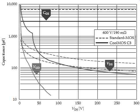
FIG. 24 Comparison of standard MOSFETs and Infineon Cool-MOS both with
190 mΩ on-state resistance.
5.2 Low-Voltage Power MOSFET
Low voltage power MOSFETs are widely used as switching transistors , for example, in AC/DC converters or DC/DC converters. Especially in the latter case, they are operated at high frequencies above 0.5 MHz making their parasitic capacitances more important as for high-voltage power MOSFETs. Also, the control losses are of higher importance since the output voltage is only a few volts higher as the control voltage and thus the relation between switched output power to needed control power is much smaller. The parasitic capacitances therefore are crucial for low voltage power MOSFETs.
To compare the performance of different low voltage power MOSFETs, the figure-of-merit on-state resistance multiplied by gate charge or multiplied by total charge are used-depending on the focus on control losses or switching losses.
Stray inductances as well as inductances on the application board and the transistor package are of high importance, because of the rather low voltage used. The fast switching leads to significant voltage drops across small stray inductances, which will influence the device behavior.
Compared to high-voltage devices where the losses are dominated by the conduction losses in the voltage sustaining layer, low voltage power MOSFETs have more leveled distribution to the on-state losses.
The impedance level in total must be lower in total, which leads to a different approach for the cell design.
The on-state resistances for the conducting inversion channel and the voltage drop over the voltage-sustaining layer are in the same order of magnitude. Additionally, the stray resistance of the package and interconnections play an important role leading to new package concepts with less parasitics; also stray inductances are reduced.
Low voltage power MOSFETs use trench gates most frequently (see FIG. 25) compared to planar gate structures dominating high-voltage MOSFETs. Trench cells allow a denser packaging of the cells, higher channel widths and thus lower channel resistances. The area of the gate electrode opposite to the drain electrode is smaller, leading to a smaller gate-drain capacitance, thus less feedback (Miller effect) and faster switching. The area of the source electrode opposite to the drain electrode also is smaller, leading to smaller output capacitances and less switching losses.
Future developments for low power MOSFETs will focus on using finer structures to improve the figure of merit R_on × Q_total.
6. Wide Bandgap Devices
SiC is well known as an ideal semiconductor for power electronic applications since several decades; however it took until 2001 to introduce the first commercial devices based on SiC into the market. The reason for this long pre-development time is the difficult substrate wafer manufacturing process. In fact, the first commercial SiC devices have been manufactured on 2 inch diameter wafer, meanwhile, only 7 years later, the wafer diameter used in production is already increased to 4. This makes the formerly exotic and expensive SiC technology much more affordable.
The unique feature of both SiC diodes and switches in the 600 V and above range is that virtually lossless switching is enabled in combination with attractive conduction behavior, allowing benchmark efficiency and reduced complexity in modern power conversion systems.
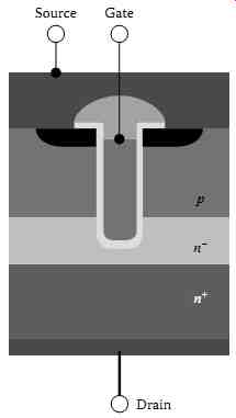
FIG. 25 Cross section through a modern low-voltage transistor.
Switching behavior @ 150°C,
IF=4A, dI/dt = 200A/μs, VR= 300 V
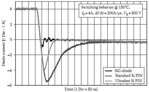
FIG. 26 Switching waveforms of SiC diode (600 V, black) in comparison
to ultrafast switching silicon diodes (gray for two 300 V diodes in series
connection, dark gray for one 600 V diode).
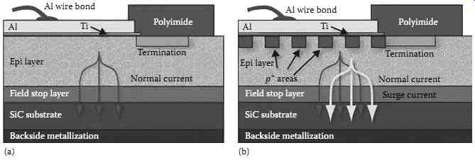
FIG. 27 Schematic drawing of a plain Schottky diode (a) and a Merged-PN-Schottky
concept (b). Carrier injection for forward voltages >3 V allow surge
current capability increase. The epi layer is responsible for the blocking
capability of the device.
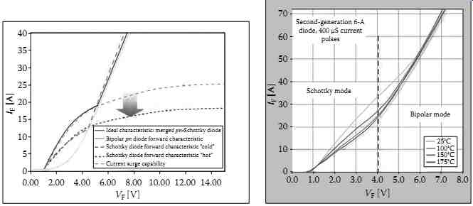
FIG. 28 Ideal (left) and measured (right) forward characteristic of
Infineon's ThinQ 2G diodes.
6.1 SiC Schottky Diodes
Other than pn-diodes, Schottky diodes don’t show any dynamic changes in the charge-carrier density, when being forward biased, as shown in FIG. 26, therefore no "reverse recovery" is also necessary when the bias changes sign. FIG. 26 demonstrates the dynamic characteristic of a SiC Schottky diode in comparison to fast-switching Si-diodes.
Based on this principle, the equivalent model of the SiC Schottky diode is very simple. It consists of an ideal diode, possessing a temperature-dependent junction potential and temperature-dependent differential resistance with no switching losses and a depletion capacitor in parallel. When switching the unipolar diode off, only the displacement current of the capacitor can be observed instead of a typical bipolar reverse-recovery waveform. As expected, there is also no dependence of this capacitive "recovery" charge (Qc) from temperature, forward current, or di/dt. Of course, such Schottky diodes can also be realized in silicon, but at a voltage rating >150 V, they suffer significantly from both very high on-resistance and leakage current. Compared to ultrafast silicon diodes, the losses depend strongly on di/dt, current level, and temperature; the SiC diodes are independent on these boundaries.
The structure of a plain Schottky diode is simple, as indicated in FIG. 27a. One of the drawbacks of this simple device is the very limited surge current capability. As the ohmic slope of its forward characteristic is purely governed by the mobility of the charged carriers (which depend via 1/T2 on temperature T), there exists a strong positive feedback mechanism between increasing current → increasing power dissipation → increasing R → increasing Vf → increasing power dissipation …, what finally leads to a thermal destruction of the devices at surge currents only ~3 times higher than rated current within 10 ms.
How can this issue be circumvented without penalty on the switching behavior? The solution is shown in FIG. 27b-it is the so-called merged pn-Schottky diode. This concept takes advantage of the wide bandgap material properties of SiC. The forward characteristic of this merged SiC Schottky diode and SiC pn diode is shown in FIG. 28. Under normal operating conditions, the high pn junction potential ( ~3 V) of SiC precludes conduction of the pn structure. Only in surge current conditions, this forward voltage will be reached, and the pn structure will provide additional carrier injection for conductivity modulation of the drift region.
The p regions with low ohmic contact to the Schottky barrier have further benefits in this structure.
They will concentrate the maximum electrical field away from the Schottky barrier surface. This allows the usage of a higher maximum field potential in the blocking mode, without degrading the barrier and compensates for the area used by the p− wells. This also provides a true and consistent avalanche breakdown characteristic-which is not achieved by competitors with plain Schottky barrier structure. As demonstrated in FIG. 28 during the normal operation (no overload), the SiC Schottky diode has a forward voltage drop of <1.5 V just as a Schottky diode and in overload (e.g., IL > 5 × IN), the diode's forward characteristic is following the SiC pn diode structure. According to this characteristic, the overload performance is just as known in the surge current operation of any pn-diodes.
Even though the p-areas shown in FIG. 27b do consume a certain area, there is no increase in the ohmic slope of the forward characteristic, as this effect is taken care for by an improved conductivity of the cell structure. The significant improvement in surge current capability comes therefore without any penalty.
Due to the very high breakdown field strength of SiC, the thickness of the required blocking layer is very small (<5 μm for 600 V SiC devices in comparison to 40-60 μm in 600 V Si-diodes). This allows even under surge current mode to ensure purely capacitive switching. FIG. 29 shows a diode commutation at a current of 10 times the rated nominal current.
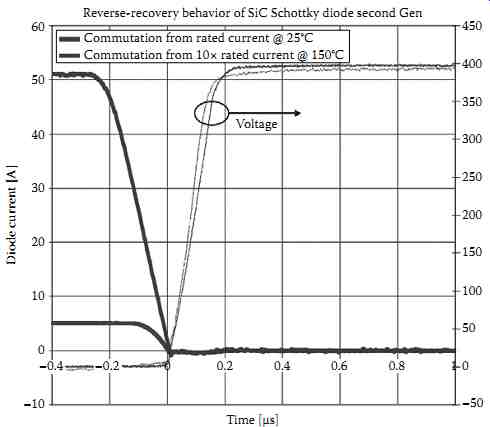
FIG. 29 Commutation of a merged pn Schottky diode from 10× surge current
at 150°C results in similar low switching losses as switching from 1x
rated current at room temperature. Further this is completely independent
from dV/dt and dI/dt.
The very small remaining capacitive switching losses are directly linked to the active area of the diode, which means that over dimensioning the SiC diode will increase those dynamic losses-this is the opposite, as what most designers are used to see for Si-diodes, where switching losses strongly depend on current density and T-rise due to self heating.
What limits the power that can be drawn from a SiC diode? With rising current, the conduction losses at full load will increase due to the ohmic behavior of the diode. The dissipated power must not drive the device into thermal runaway nor violate max junction temperature ratings. With the merged pn/Schottky concept, we get already a nearly temperature-independent forward characteristic (as can be seen from FIG. 29, right-hand graph beyond at Vf of 5.5 V), which practically eliminates the problem of thermal runaway. For the reduction of junction temperature, an appropriate mounting technology is required, which takes away the thermal barrier from the 60 to 80 μm thick solder layer being conventionally used for mounting power devices into discrete packages.
In effect, the extremely good thermal conductivity of SiC is now directly coupled to the large and also good thermal conducting copper lead frame of the TO package. The conventional solder layer is replaced by an extremely thin diffusion zone that is only 2 μm wide. This results in a significant improvement of both steady-state thermal resistance Rth and transient thermal impedance Zth.
Of course, SiC Schottky diodes are not limited to 600 V. Due to the comparatively low resistivity of the necessary blocking layers ("drift layers"), 1200 and 1700 V Schottky diodes have very attractive performance values in comparison with their Si counterparts. As for the 600 V level, the switching losses are only minimal and are due to capacitive displacement current. In fact, the capacity of 1200 V with a certain active area is even smaller than for a 600 V device, caused by the lower doping concentration in the drift layer. Thus, those diodes are ideal companions as freewheeling diodes for modern ultrafast Si- IGBTs.
6.2 SiC Power Switches
Even after 9 years of commercial availability of SiC diodes, there still is no SiC power switch in the market. The reason is surely not that such a device would not have plenty of application benefits.
This is especially true in the voltage range of 1000 V and above, where unipolar switching devices like Si-MOSFETs are already very rare and of insufficient performance (best in class discrete devices have typically several Ohm on resistance). The main competition in this voltage range comes from IGBT-like devices, with their well-known restrictions with respect to switching losses and maximum frequency.
Thus, many application engineers are looking for SiC-based alternatives for applications like solar converters, UPS, HEV, and high-precision drives.
There have been plenty of announcements of achievements made on SiC switches in the recent years, but no products have materialized. There are various reasons for this, but for sure one dominating issue is the insufficient quality of the SiC oxide interface. A SiC MOSFET suffers not only from a low channel mobility, which compensates a big part of the advantages of the physical properties of SiC, but also the reliability of the SiC MOS system with respect to the so-called extrinsic (early) failures is still questionable.
However , for the time being there is one device in favor, a so-called junction field effect transistor (JFET) power switch concept in SiC, which does not require a gate oxide and offers superior ruggedness in many application aspects (e.g., ESD, electrostatic discharge-ESD, avalanche, short-circuit conditions). However, this device is normally on (conducting without gate voltage), when best cost/ performance is the target. This feature can be addressed with the help of a cascode configuration employing a low voltage MOSFET to generate the necessary voltage drop along the MOSFET source-drain path to pinch the JFET off. This principle is shown in FIG. 30. For the SiC-JFET, very attractive area-specific on resistances have already been achieved: <6 M Ohm × cm2 for devices with 1200 V blocking.
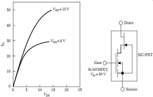
FIG. 30 Schematic of a high voltage SiC-JFET/low voltage Si-MOSFET
configuration (right). The output characteristic of this cascode is equivalent
to the low voltage Si-MOSFET, whereas the blocking properties are determined
by the SiC-JFET.
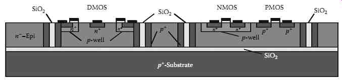
FIG. 31 A PIC cell in SOI technology showing a power MOSFET and standard
CMOS MOSFET.
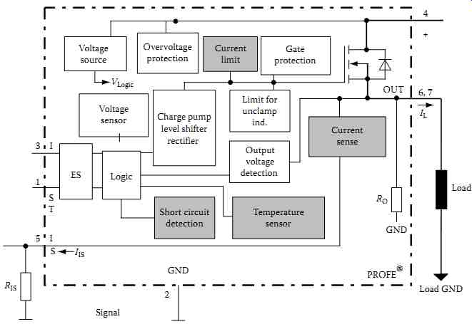
FIG. 32 Block diagram of a fully protected high side switch.
7. SMART Power Systems
Considerable challenges that system engineers are frequently faced with are the device selection, control functions, and the optimized operation along the SOA-diagram (Save Operating Area), together with the implementation of protective and diagnostic features in power semiconductor components. This problem has been solved with IC-compatible power switches, the so-called SMART-Power systems. These new generation of power semiconductor switches have integrated all the controlling protection and diagnostic-functions together with a communication interface on one chip. Depending on the power rating (voltage capability and current scaling), circuit complexity, and requirements toward safety isolation, there are several ways of realization , for example, monolithic integration in SMART power technology (SPT) or silicon on isolator (SOI), chip-on-chip (CoC), chip-by-chip (CbC) or multi-die assembly on substrate carriers.
In this new generation of devices, microelectronics and power electronics are combined for both systems and manufacturing. This has triggered a new area in system integration of power and microelectronics, a significant step toward system miniaturization, higher reliability, reduced dissipated power, and fully protected and communicable electrical systems. A broad spectrum of various semiconductor technologies for "SMART" solutions has been developed since the mid-1980s.
7.1 High-Voltage System Integration
In typical power conversion systems , for example motor control, the input voltage (supplied by the mains) has to be rectified and the output would be controlled to optimize power transfer for varying motor load conditions. There is a great demand expected for such electronic motor drive systems for domestic appliances that are required to meet energy efficiency guidelines. In such mass market consumer applications, economy of scale can be achieved by reducing electronic component count in the overall electronic systems.
Since these system solutions are entire power electronic circuits comprising a full bridge diode rectifier, IGBT converter and gate drive circuit can be integrated. For such integration, lateral power switching devices such as lateral IGBTs or power MOSFETs (LDMOS, FIG. 31) with all there terminals on the surface have to be used. The technology that is most promising for such integration is SOI, which allows total static isolation between power devices. FIG. 31 shows the integration of various power devices using trench isolation.
7.2 SMART Power Technology for Low-Voltage Integration
Until the mid-1990s, bipolar technology was the dominant process for power IC's. Depending on their breakdown voltage, these processes could only offer a limited element density. The maximum power dissipation is restricted by the base current and the saturation voltage of the bipolar power transistors.
SMART power processes overcome these limitations. Analog functions can be realized with bipolar transistors, CMOS logic allows complex logic functions, and DMOS power transistors result in negligible power dissipation. Technical requirements of the application and general cost considerations restrict the choice of the optimum process , for example in selecting self-isolation or junction isolation, SMART-power technology.
The number of power output channels is a relevant orientation for the structure of the power transistor and this decides on the technology. In case of single output, the backside of the chip can act as the drain contact, which stands for self-isolation technology. Thus, the current flows vertically through the devices, which is optimal for the power losses generated. For multiple outputs, all contacts are normally placed on top of the chip and as a consequence, the current flows laterally. In this case, the junction isolation process is the favorite.
SMART power technology in self-isolation technologies is preferred for high current devices-the voltage rating is typically <100 V. The backside of the power MOSFET chip is used as the common drain of a single or multiple power DMOS transistor(s).
Various protection functions are included in the element-monolithically or in CoC-technology-and are indicated by the status output , for example, over-temperature, short circuit, open load, over- and undervoltages shutdown, reverse polarity, load dump protection, communication enforce, etc. (FIG. 32).
For highly complex logic functions, CMOS technology is the best choice. Analog circuits can be fabricated in bipolar, and any number of separate DMOS power transistors can be integrated. If the application requires high logic density, multiple channels (as high-side or low-side switches), and moderate output power, the junction isolations technologies is the most suitable way for system integration.
8. Summary
For all power electronic systems to be realized, it’s essential to be able to actively control the dynamic power transfer in all optimum manners. This can only be achieved through the use of the optimized electronic switching devices. For extremely high-power applications, the bipolar devices , for example, thyristors, LTTs, and IGCTs, including their future development are the driving technology today and in the next decades.
The high-power and medium-power system development will be dominated by the IGBT. A huge potential for further development is given. All applications requiring high and ultrahigh switching frequencies in order to minimize the power electronics converter at high energy efficiencies are driven by Power MOSFETs. For lower voltage (<100 V) as well as high voltage (>500 V), many advances have been made; new generations will follow.
All innovations in the car will be driven by SMART-Power systems. This technology covers power switches with simple logic functions integrated up to highly sophisticated system solutions with low power output stages.