AMAZON multi-meters discounts AMAZON oscilloscope discounts
Today's products can contain hundreds or even thousands of components. Even after you've considered a unit's failure history and pondered a preliminary diagnosis, there can still be lots to examine and test. How the heck do you find your way around what looks like a city on Mars? There are three types of roadmaps to help you navigate the innards of an electronic device:
Block diagram • This lays out the device by the function of each section and its basic interconnections. It does not show individual components or specific connection points. It's the most general, conceptual view, analogous to a map showing cities and route numbers for major highways between them, but not street-level detail. See FIG. 1.
Schematic diagram • This shows all the components and interconnections but does not indicate their purposes by specifying sections or overall structure. This is the street-level map. See FIG. 2.
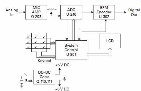
FIG. 1 Block diagram
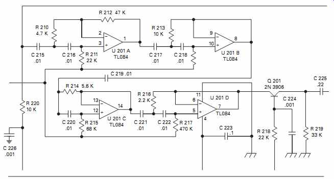
FIG. 2 Section of a schematic diagram
Pictorial diagram • This uses drawings of the parts and shows their interconnections. The pictorials included in service manuals are really layout diagrams, detailing the placement of components as they exist on circuit boards and chassis. This is the drawing of landmarks and where to find them. See FIG. 3.
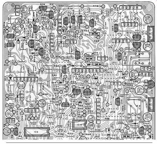
FIG. 3 Pictorial diagram
All three diagrams work together to guide you to your destination. The block diagram helps you grasp the signal flow and interactions between circuit sections so you can see how they are supposed to work with each other. The schematic shows you individual components and stages so you can zero in on specific components you may want to scope or pull for testing. The pictorial helps you find the darned things! If you can obtain only one style of diagram, get the schematic, because it offers the detail necessary for troubleshooting at the level of individual components. In years gone by, most products included a schematic, printed inside the case or in the instruction guide. That became impractical as gadgets got more complex; there were just too many parts to fit the diagram in such a small space. For awhile, manufacturers supplied fold-out schematics with their instruction guides, but they finally began omitting the sheets as products no longer had incandescent lamps, snap-in fuses or any other parts the user could change. After all, only a service tech could really make use of diagrams anyway, so why spend the money to print them by the hundreds of thousands? Instead, service manuals were made available to repair shops, and the end user, soon to be called the "consumer," was left high and dry, no longer privy to the products' insides. "No user-serviceable parts inside. Refer service to qualified personnel," replaced the diagrams. Is it any wonder they call today's gadgetry "consumer electronics"? Service manuals were cheap and plentiful, and shops kept huge rows of filing cabinets bursting with them. In addition to manuals generated by the products' makers, the Howard W. Sams company produced its own comprehensive line of Photofact schematics for just about everything out there. If you couldn't get a schematic from Zenith, you could get a Sams easily enough for a buck or two.
As products got still more complex, manuals grew from a few pages to a few hundred, with large, fold-out schematics and very detailed, color pictorials. Producing these big books became quite expensive, so their prices skyrocketed. Shops continued to buy them-they had little choice-but no consumer would spend more for a manual than the product cost in the first place! Companies gradually reduced and finally abandoned the infrastructure for selling manuals to the public, and today's age of "use it, wear it out and toss it" was in full swing. Many manufacturers will no longer sell schematics or service manuals to consumers, thanks in part to fear of potential lawsuits by injured tinkerers. Some companies won't even sell manuals to service shops unless they're factory-authorized warranty service providers. And, believe it or not, some even refuse to provide diagrams to those facilities! Secretive computer makers, in particular, only let authorized servicers swap boards; the techs work on their machines for years without ever seeing a schematic of one.
Where does this leave you? Forget calling the major manufacturers; they won't sell you a service manual no matter how you plead. There are online sources, though, continuing to provide this vital information, at least for some products. Howard W. Sams continues as Sams Technical Publishing, at www.samswebsite.com. Their Photofact and Quickfact manuals aren't $1.50 anymore. As of this writing, most of them cost $20 and up. Still, for a tough case that has you going around in circles, it may well be worth the investment. Numerous other sites offer diagrams, some for free. Doing a Web search may turn something up, and it's always worth a try.
Schematics and Concepts
Reading a schematic is a bit like reading music: learning to name the notes is just the beginning. To really understand what's going on, you need to recognize the larger harmonic and rhythmic structures and how individual notes fit into and connect them. Identifying components on a schematic is a good start, but seeing how they form stages and sections, and how those work with each other, is vital to being able to find the ones that aren't properly performing their functions. The best techs have a good grasp of circuit fundamentals, but there's no need to be an engineer or a math whiz. It's far more useful to be familiar with the overall structure and with how basic circuit elements like transistors work.
In Section 7, we reviewed the component symbols for the most common parts.
Along with those, schematics include symbols for other items. Here are some you're likely to encounter:
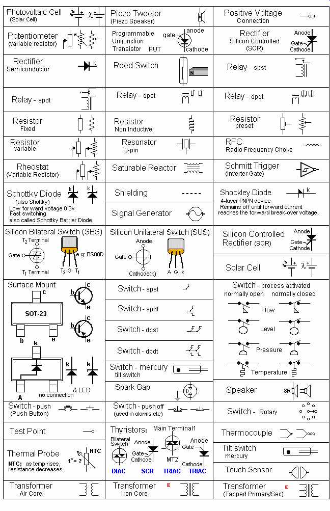
AC Voltage The presence of AC voltage is indicated by a sine wave. Antenna The antenna symbol represents any type of antenna, even if it doesn't resemble the symbol.
Battery In addition to the main batteries powering portable devices, small backup batteries may be found on circuit boards, either soldered or in holders. When wires connect batteries or battery holders, it is standard to use a red wire for positive and a black wire for negative.
Conductors, Joined This is where two wires or circuit traces meet and connect.
Conductors, Not Joined This is where two wires or circuit traces cross on the schematic (but not necessarily physically in the device) without connecting.
Older schematics use the 3D-looking loop shown on the right. Newer diagrams don't, because today's products are so densely packed with interconnections that the loops become unwieldy and take up too much room on the schematic. Remember, if there's no dot where they cross, they are not connected! When a conductor meets another one without crossing, though, it is connected whether or not there's a dot.
Conductors, Merged This shorthand description of multiple wires is widely used in digital gear, particularly when parallel data lines all go to the same chip. Instead of showing a separate conductor for each line, only one is shown, making complex schematics a little less cluttered and a bit easier to read.
DC Voltage The lines represent what DC looks like on an oscilloscope, with the dotted line indicating ground.
Ground There are four types. Earth (at left in the illustration) indicates a connection to the AC line's ground lug. Chassis (at right) means the connection goes to the unit's metal chassis or, lacking one, a common point on the circuit board. The earth symbol is often used in place of the chassis ground symbol-you'll see it in battery-operated gear that never gets connected to the AC line-but not the other way around.
Analog and digital ground symbols are used in devices having separate ground points for their analog and digital sections. This arrangement helps keep electrical noise generated by the digital system from intruding into sensitive analog circuits. Many CD, DVD and MP3 players have separate analog and digital grounds. In some products, the grounds meet, and only the length of a circuit board trace separates them. In others, analog and digital grounds remain separate, and connecting them externally will cause malfunction or undesired noises in the output signal.
Jack There are many styles of jacks, so jack symbols are somewhat pictorial. Also, some jacks have internal switches that sense when a plug is inserted, and those will be shown too.
Speaker The speaker symbol looks like a classic loudspeaker, but it can be used to indicate headphones as well. Sometimes a drawing of a headset will be shown instead.
Call Numbers Each component will have a part number unique to that product's schematic. Some techs refer to it as the call number. That number is unrelated to the part number printed on the component, the one by which you can look up the part and learn its electrical characteristics. Instead, the call number is derived from the parts list found in the service manual.
Each call number begins with a letter specifying the type of component, followed by a few numbers. The first number tells you in what section the component resides, and the others are unique identifiers. Designations like R201, L17 and Q158 are call numbers.
The section number is arbitrary and varies from product to product, but parts with the same first number will live in the same neighborhood. For example, R201, Q213 and C205 will all be in the same area, but R461 and Q52 won't. And C206 is probably right next to C205, or at least not very far away. If the circuit board is labeled, it'll show those numbers next to each component.
Every part normally has its own call number, but multisection integrated circuits such as op-amps may be shown with each section as a separate device, even though they're really in one package. In FIG. 2, the TL084 chip has four sections, each labeled A, B, C or D. On another schematic, the same component could be drawn as one rectangle resembling the shape of the real thing, with all four sections inside. In that case, each section's triangular op-amp symbol might be drawn inside the little box, but you can't count on that. Presenting the part as separate sections helps keep the signal flow clearer and is the preferred method.
Although each schematic has unique call numbers, the component type letters are somewhat standardized. Here are the letters in common use:
===
Component Designator Component Designator
Capacitors C Relays RL Connectors J or CN Speakers SP Crystals and resonators X or Y Switches S or SW Diodes D Transformers T Fuses F Transistors Q Coils (inductors), but not transformers L Test points (places to put your probes) TP Integrated circuit chips IC, U or Q Voltage regulators IC, U or Q Resistors R Zener diodes Z, ZD or D Potentiometers R or VR
Because Q is the designator for transistors, it gets used for just about anything made from them, even if they are microscopic structures in an integrated circuit chip.
Newer schematics, though, are more likely to differentiate, calling integrated circuits U, transistors Q, and voltage regulators IC.
==
Call numbers are handy even if you don't have a parts list, because they help you identify mystery components. Especially in this age of ultra-tiny, surface-mount parts, some look so similar that it's hard to guess what they are. If you see a call number starting with an R, you know the part is a resistor. An L tells you it's an inductor, and so on. Should you run into a part with a designator not covered in this guide, a quick trip to the Internet will turn up its meaning.
The Good, the Okay, and the Awful
Not all schematics are alike. There are good ones, even great ones. There are average ones. And there are the dreadful diagrams that are almost worse than none at all.
The Good
A good schematic is logically laid out, showing most stages with signal flow from left to right, with enough space between the stages to make the organization clear. It includes call numbers and part numbers, with resistor and capacitor values specified.
A really good one may have arrows indicating signal flow through and between stages. A truly great diagram even has voltage readings and--it doesn't get better than this--snapshots or drawings of scope waveforms at various test points! If you're lucky enough to work with such a schematic, it'll greatly speed up your hunt. Touch a probe, compare what you see to the diagram, and either it looks the same or it doesn't. In real life, it's rarely as simple as that, but having those guideposts is a wonderful help.
The Okay
A merely okay diagram is clear, with a reasonable sense of organization. It has call numbers but probably no part numbers or parts values. Forget about signal flow arrows or waveforms. It's no GPS, but it's a serviceable roadmap. Everything is accurate and nothing is left out. Which brings us to the dark side, that malevolent maw of misleading misery, the incorrect schematic.
The Awful
A really bad schematic may have reversed diode polarity, wiring errors, incorrect connection indications on conductors crossing each other, or omission of some parts, any of which can confuse the living heck out of you and send you off in the wrong direction. Switches show no indication of what they do in what position, and the drawing might not even be clear enough that you can read parts of it. Still, even a miserable schematic can be better than none, as long as you remember not to trust everything you're seeing. Occasional errors crop up in even the best diagrams, of course, but it's rare to find a truly rotten schematic from a major manufacturer. I've seen some doozies from off-brand companies, though.
Schematics for Novices
To get started reading schematics, consider the organization of a guide. It begins with letters that form words, which make sentences. Those are grouped into paragraphs and finally into Sections. Each paragraph links with the others to tell a story, and the Sections present a progression driving toward the finish. Some conditions are introduced at the start of the guide and resolved at the end.
Electronic devices are organized much the same way. Components work together to form stages, each one feeding others, resulting in a signal flow proceeding from some starting point, such as a microphone, antenna or DVD, to some ending point, perhaps a display screen or a speaker. Each stage performs a function contributing to the overall processing. A group of stages involved in a particular part of the device's operation constitutes a section dedicated to a specific purpose.
With occasional exceptions, a schematic's signal flow in each stage proceeds from left to right. Signal flow between stages normally goes left to right as well. So, the most sensitive stages handling the weakest signals are usually on the left side of the page.
If you're looking for an antenna or microphone input, look for it there. In a power supply, the AC line connection is probably on the left side, too, as it's considered the supply's input. Very complex schematics sometimes violate these conventions, simply because they run out of room on the page.
Look for power supply sections at the bottom of the page. Output sections, LCD screens and speakers should be on the right. Processing stages, such as the IF (intermediate frequency) stages of a radio receiver or the microprocessor in an MP3 player, will be in the middle.
When reading a schematic, keep your eye on the story and its central characters.
Not all players are equally important. The plot is driven by the active elements like transistors and ICs, since they do most of the work. Crystals and resonators generate signals, so they're crucial characters, without which the story never gets moving.
After those, look for coupling elements such as transformers, capacitors and resistors linking one stage to the next. They move the plot forward, because signals will be flowing through them on the way to subsequent stages. The other resistors, capacitors and coils set the voltages, currents and various conditions the big shots need to do their jobs. Those subplots are necessary to the overall story but not central to its theme. Try not to let them distract you from the primary action. Let's look at the schematics of a few circuits and how to interpret them.
Amplifier Stage
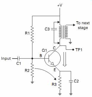
FIG. 4 Amplifier stage
For our first adventure, we'll look at a single stage. Let's examine every part in it, what it does and what would happen if it malfunctioned.
This one is an inverting amplifier, typical of what you might find in just about any product. See FIG. 4. Inverting means that the output signal rises as the input signal falls, and vice versa, producing a replica that's upside down. Sometimes inversion is necessary to the circuit's operation, while other times it's just an irrelevant consequence of getting voltage gain from the stage. Either way, you'll see lots of inverting amplifier stages.
The stage has four major points where things go in and out. At the top, power is applied through the transformer, reaching the collector of the transistor. Signal input is on the left and goes to the base of the transistor, Q1, via C1. The output is at Q1's collector, which is why TP1, the test point, is there. Finally, R2, R3 and C2 go to ground. Ground is as important an input/output point as the others; without ground, you've got a paperweight.
To be a sharp troubleshooter, you need to understand how the circuitry is supposed to function. So, let's see how this thing works, starting at the top. Power goes through the winding of the transformer and reaches the collector of the transistor, Q1.
It's the active element, so it's the central character. When the transistor is turned off, no current passes through the transformer, because the lower end of its winding sees no connection to ground. When the transistor is turned on, the path between collector and emitter connects, effectively grounding the transformer's winding and completing the circuit, pulling current through the winding.
It's not an all-or-nothing proposition, though. Remember, transistors act like variable resistors (potentiometers), except that signals, rather than your fingers, turn them up and down. Here, the signal is applied to Q1's base through C1. C1 couples only the AC component of the incoming signal to Q1, preventing any DC in the signal from reaching the transistor, and also preventing any DC from Q1 getting back into the previous stage.
Where R1 and R2 meet establishes a voltage somewhere between the power supply's value and ground, to bias the transistor's base, or put a little DC on it, keeping it turned on through whatever portion of the incoming signal's waveform the amplifier is intended to amplify. As with most amplifiers, we want the whole waveform, so the transistor has to be biased with enough positive current that when the incoming signal goes negative, the transistor's base never gets below about 0.6 volts, which is the cutoff point for a standard bipolar silicon transistor. The bias current has to flow through R2, so its value determines how much is available to the transistor's base; the higher R2's resistance, the less bias current there will be.
The transistor passes current from collector to emitter in proportion to how much current passes from base to emitter, as shown by the arrows. The ratio of the two currents determines how much the transistor can amplify a signal. It is an inherent part of the component's design and is given in its specifications. As the incoming signal wiggles up and down, the base current varies with it, causing the transistor to pull a proportionally larger current through the transformer on its way to R3 and finally ground. That forming of the power supply's DC into an enlarged replica of the signal is called gain and is the essence of amplification and the foundation of all modern electronics, analog or digital.
Ah, R3 and C2. What're they there for? R3 limits the total current through the circuit; without it, the transistor would attempt to pull the power supply's entire current capability to ground, dragging down the supply and probably blowing the transistor or the transformer. R3 limits the total base current as well, because it's in series with that path too. Thus, it sets a limit to how much signal current the previous stage has to supply.
C2 is a little trickier to explain. Transistors, having adjacent regions of semiconductor material in them that are not at the same voltage at the same time, also behave like capacitors. They store some charge and take a little time to discharge.
The presence of R3 slows that down because the discharge has to reach ground through its resistance. This forms a time constant, which is a fancy way of saying that there's an upper limit to how fast the transistor can get rid of its charge. The bigger the value of R3, the longer the discharge process takes, and the slower the transistor can react to incoming signal changes. When the frequency of the incoming signal is faster than the time constant, the transistor's residual charge fills in as base current drops, acting like any filter capacitor and smoothing out the waveform. As a result, the transistor can't react quickly enough to respond and amplify the signal. Thus, the upper speed limit, or frequency response, of the amplifier drops off.
C2 allows the rapidly changing parts of the signal to reach ground with less resistance, discharging the transistor faster. The apparent resistance of a capacitor drops with increasing frequency, because it never gets the chance to charge fully and oppose the incoming current. So, C2 compensates for the transistor's capacitance, giving it a lower-resistance path to ground with increasing signal frequency. The result is to restore the lost high-frequency response of the amplifier without also increasing the low-frequency response.
T1, the transformer, plays a crucial part in the amplifier's operation. As current is pulled through its primary coil, it generates a magnetic field that impinges on, or cuts across, its secondary coil, the one on the right. As the current in the primary gets stronger and weaker in step with the signal, the changing magnetic field generates a current in the secondary that makes its voltage rise and fall in step. That changing voltage couples the new, amplified signal to the next stage. There are other ways to couple a signal, without a transformer, but using one has advantages in some kinds of circuits, especially those employing the transformer as a tuned circuit resonating at a specific frequency. Radio receivers use lots of tuned amplifiers of this sort to pick out the selected signal from all the others hitting the antenna. A capacitor across the transformer, shown in FIG. 4 by the optional C3, is a dead giveaway that an amplifier is tuned. C3 could be on the other side of the transformer, too, and still have the same effect in tuning it to a desired frequency.
Malfunctioning Parts
Now that we've explored how the amplifier stage is supposed to work, let's see what the effects of malfunctioning parts would be. Again, starting at the top, how would a bad transformer affect the performance of the circuit? If the transformer were open, no current would pass through its primary, so the collector of the transistor would read 0 volts. Transformers in small-signal circuits don't pass much current, so an open winding is unlikely, but it can happen. By the way, to estimate how much total current the winding might have to handle, just divide the power supply voltage by the value of R3, a la Ohm's Law. This pretends that the transistor and the transformer's winding have no resistance, so the real value will be a bit less, but at least you'll know the approximate upper limit.
If the transformer had a short, its resistance would decrease and it'd be harder for the transistor to pull its lower winding connection toward ground, so the voltage at the transistor's collector would be close to that of the power supply, with little signal variation. Depending on the total current through the circuit (limited by R3, as described above), the transistor might get hot or even be blown.
If R1 were open, there'd be no bias current going to the transistor's base, so the transistor would be turned off. Its collector would be at the same voltage as the power supply, and its emitter would be at ground potential, 0 volts. The signal itself might have enough current to turn the transistor on a little bit during the positive half of its waveform, resulting in a weak, distorted mess of negative-going signal excursions appearing at its collector. (Remember, the amplifier inverts.) Shorted resistors are pretty much unheard of, but, for the sake of this thought experiment, we'll consider what would happen if one did short. If R1 shorted, the base would be biased to the power supply's full voltage. The transistor would be fully turned on no matter what the incoming signal did. The collector would read somewhere close to 0 volts, and the transistor might be hot, as might be R3.
If R2 were open, the bias would be too high, with much the same result. The signal's influence might result in some output, though only on the negative-going half of its waveform. Those negative incoming peaks would cause a rise at the output, thanks to the inversion. As before, you'd get a weak, distorted mess, but the collector's DC level would be low, not high.
If R2 were shorted, the base would be pulled down to 0 volts, resulting in the same no-bias conditions you'd get if R1 were open, except that the signal could not produce any output at all, because it would be shorted to ground as well.
If C1 were open, no signal would get to the transistor, but the DC voltages on Q1 would look just fine.
If C1 were shorted, the base bias would be influenced by the previous stage, resulting in unpredictable behavior. If the bias were pulled toward ground, Q1's collector would rise, clipping off the top of the output signal if it got too high. If the bias went high because of voltage being fed in from the previous stage, the transistor would turn on too hard, the collector would be low, and the signal would be cut off toward the bottom.
A shorted or leaky input coupling capacitor is something you might actually run into, particularly when it's an electrolytic or tantalum cap. With a leaky one, it can be maddening to try to deduce why the stage behaves so oddly. If you disconnect the input cap and the DC voltages on the transistor change, the cap is letting some DC pass through it. It's leaky.
Now to the heart of the stage: the transistor. This is the component most likely to cause trouble. Transistors can fail in numerous ways. They can open from emitter to collector, usually as a result of overcurrent. They can also short that way, and often do. A short or an open can occur from base to emitter as well. I've seen transistors with all three leads shorted together like one big piece of wire! Transistors can be leaky, too, allowing current to pass when it should be cut off, or even to move backward through their junctions. A very small amount of reverse leakage is normal, actually, but it's not enough to affect the circuit's operation. A leaky transistor allows much more reverse current, and that'll produce all kinds of unpredictable effects. The little monsters can also become thermal, changing their gain and leakage characteristics as they warm up.
An open between any two junctions will result in no output. TP1 will be at the power supply voltage, because the transistor will not pass any current toward ground.
Even if the collector-emitter junction is fine, an open base junction will prevent the transistor's being turned on.
A shorted collector-emitter junction, which is quite common, will appear as if the transistor were turned on all the time, all the way. The collector voltage will be at or very near zero. A shorted base-emitter junction, also common, will pull the base bias and incoming signal down toward ground through R3, and the transistor will not turn on. So, the collector voltage will not pull down and will be at the power supply voltage. A short from collector to base will turn the transistor on, having the opposite effect.
A quick-and-dirty way to hunt for transistor shorts is to check the DC levels on all three leads. If any two are exactly the same, the part may very well be shorted. If they're even a little bit different, a short is far less likely.
If a transistor has leakage, it can act strangely. If collector current flows into the base, for instance, it can overbias the part. Depending on how much current leaks, the transistor may still work to some degree. If a stage acts wonky but everything seems to measure okay, and especially if the behavior changes with temperature, leakage is likely.