AMAZON multi-meters discounts AMAZON oscilloscope discounts
...
1 Introduction
At the turn of the century, around 75% of the power generated was processed by power electronics. In the modern scenario of electronics, ultra-large-scale integrated (ULSI) circuits, which progress toward system-on-a-chip (SoC) concepts, are powered by DC power rails as low as 1.2-0.7 V. These two scenarios have made the demands within the power conversion interface complex. Compact ultra-low-DC voltage sources with energy backup, fast transient response, and power management have become mandatory in powering modern electronics. Uninterruptible power supplies and advanced power conditioning with surge protection have become essential in providing clean and reliable AC power.
Modern electronic systems are uniquely vulnerable to power line disturbances because they bring together the high-energy power line and sensitive low-power integrated circuits controlling power semiconductors in the AC-to-AC conversion interfaces as well as the DC-DC converters. The term power conditioning is used to describe a broad class of products designed to improve or assure the quality of the AC voltage connected to sensitive electronic systems.
Utilities realize that different types of customers require different levels of reliability, and make every effort to supply disturbance-free power. However, normal occurrences, most of which are beyond control and are acts of God, make it impossible to provide disturbance-free power 100% of the time. In addition to these external disturbances, sources within buildings, such as switching of heavy inductive equipment loads, poor wiring, overloaded circuits, and inadequate grounding, can cause electrical disturbances.
Many of these power disturbances, particularly the transient surges, can be harmful to sensitive electronic equipment with low-voltage DC power supplies. Power disturbances can cause altered or lost data and sometimes equipment damage, which may, in turn, result in loss of production, scheduling conflicts, lost orders, and accounting problems.
There are methods and devices available to prevent these disasters from happening.
Protective systems range from those providing minimal protection to those that construct a new power source for critical loads, converting the standard "utility-grade power," which may be adequate for most equipment, into the "electronic-grade power" required by many critical loads. This Section discusses the protection against transients and surges in power conversion systems required for electronic systems demanding 99.999% or higher reliability. Treatment will be on a low-voltage electronic circuit protection basis only, and hence a discussion on power-engineering aspects is not treated in the Section.
2 Types of Disturbances and Power Quality Issues
In a single- or three-phase utility power supply, commercial power companies are expected to supply AC power at a nominal RMS voltage with a percentage tolerance such as ±6% with limited amounts of harmonics as per applicable standards. However, the practical utility grade power supply carries many unwanted RMS voltage disturbances, harmonics, noise, and transients. Figures 9.1(a) and 9.1 (b) depict the RMS voltage disturbances and transients and noise. FIG. 1(c) indicates the case of a 50 Hz, 230 V RMS power supply and its corresponding frequency spectrum.
2.1 RMS Voltage Fluctuations
2.1.1 Voltage Surges
Voltage surges are voltage increases that typically last from about 15 milliseconds to one-half of a second. Surges are commonly caused by the switching of heavy loads and power network switching. Surges don't reach the magnitudes of sharp spikes, but generally exceed the nominal line voltage by about 20%. This kind of deviation can cause common computer data loss, equipment damage, and erroneous readings in monitoring systems.
A surge that lasts more than two seconds is typically referred to as an overvoltage.
2.1.2 Voltage Sags
Voltage sags are undervoltage conditions, which also last from 15 milliseconds to one-half of a second. Sags often fall to 20% below nominal voltage and are caused when large loads are connected to the power line. Sags can cause computer data loss, alteration of data in progress, and equipment shutdown. A sag that lasts for more than two seconds is typically referred to as an undervoltage.
2.2 Transients
As depicted in FIG. 1(b) voltage transients are sharp, very brief increases in the supply waveform. These spikes are commonly caused by the on and off switching of heavy loads such as air conditioners, electric power tools, machinery, and elevators. Lightning can cause even larger spikes. Although they usually last less than 200 microseconds, spikes can be dangerous to unprotected equipment, with amplitudes ranging from about 180% of the peak value to over a few thousands of volts, positive or negative, and sometimes as high as 6000 V or even larger. This high magnitude of sudden voltage variations can wipe out stored data, alter data in progress, and cause electronic-hardware damage.
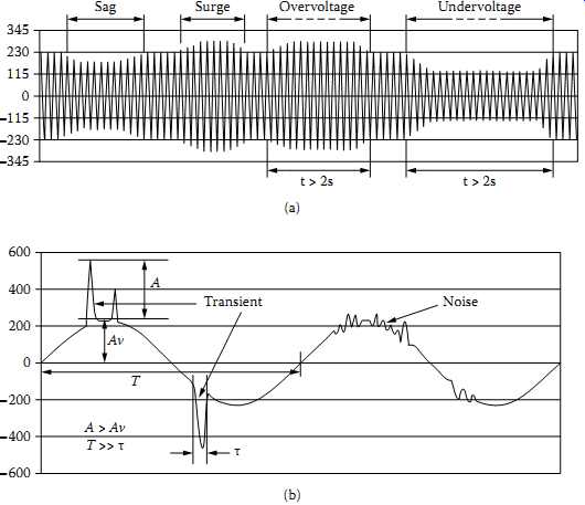
FIG. 1 Examples of disturbances on a 230 V RMS, 50 Hz utility AC power supply:
(a) RMS voltage fluctuations; (b) transients and noise superimposed on the
waveform; (c) ideal waveform and its frequency spectrum.
2.3 Electrical Noise
Electrical noise is a high-frequency interference in the frequency spectrum of 7000 Hz to over 50 MHz. Noise can be transmitted and picked up by a power cord acting as an antenna, or it can be carried through the power line. These disturbances can be generated by radio frequency interference (RFI) such as radio, TV, cellular, and microwave transmission, radar, arc welding, and distant lightning. Noise can also be caused by electromagnetic interference (EMI) produced by heaters, air conditioners, white goods, and other thermostat-controlled or motor-operated devices.
Although generally nondestructive, electrical noise can sometimes pass through a power supply as if it were a signal and wipe out stored data or cause erroneous data output. Problems result when microelectronic circuitry is invaded by transient, high frequency voltages collectively called "line noise," which can be grouped into one of two categories: normal mode or common mode (described later).
2.4 Harmonics
Harmonic distortions are usually caused by the use of nonlinear loads by the end users of electricity. Nonlinear loads, a vast majority of which are loads with power electronic devices, draw current in a nonsinusoidal manner. With the increased use of such devices in consumer loads, the presence of distortions in current and voltage waveforms has become a frequent occurrence today. For instance, virtually all modern computer power supplies use a direct rectification mode of AC input to derive a bulk DC power supply for conversion into lower DC rails using switch-mode techniques. A simple example is illustrated in FIG. 2. Since the rectifiers can conduct only when the instantaneous line voltage is higher than the smoothing capacitor voltage, the charging of capacitors takes place only during a small time period, resulting in narrow input current pulses as shown in FIG. 2(b). Referring to FIG. 2(c), if any one or several of the loads connected to the distribution bus draws a nonlinear current, terminal voltage at the consumer terminal will be a distorted sinewave. It’s quite common to have a flattened-top sinewave due to non-linear loads such as computer power supplies, UPS rectifiers, or even energy-saving lamps. The ultimate result is that the terminal voltage at the consumer end will be a nonsinusoidal waveform with lot of harmonics.
In view of the widespread use of power electronic equipment connected to utility systems, various international agencies and national agencies have proposed limits on harmonic content injected into the system.
2.5 Modes of Transients and Noise
The noise and transients sources superimposed on the utility voltage can come in two different forms, namely common mode and differential mode. Differential mode is sometimes also referred to as normal mode or transverse mode. In tackling surge protection in power electronic systems, it’s very important to deal with both cases.
FIG. 3 indicates the two cases.
2.5.1 Differential Mode ( Normal Mode or Transverse Mode)
As the name implies, differential-mode signals appear between the live wire and the accompanying neutral for a case of AC supply input. Similar to a DC power supply, it means the positive or negative rail and its return current path. These two lines represent the normal path of power through the electric circuits, which gives any normal-mode signal a route into sensitive components.
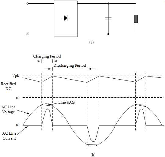
FIG. 2 Distortion of the voltage waveform due to nonlinear loads: (a) simple
case of bridge rectifier; (b) rectifier input current in relation to input
voltage waveform; (c) simplified case of distribution bus, with a sinusoidal
generator, and linear bus impedance before the point of common coupling (PCC).
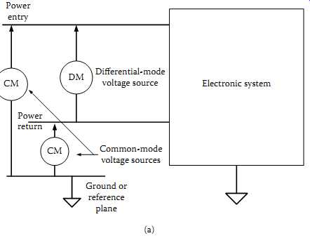
FIG. 3 Different modes of signal inputs and the effect of isolation transformer:
(a) differential and common modes; (b) common-mode signal coupling toward
secondary side due to coupling capacitance. ((a) (b) Differential-mode voltage
source Common-mode voltage sources Ground or reference plane Power entry Power
return CM DM CM; Electronic system Primary Secondary)
2.5.2 Common-Mode Signals
Common-mode signals are voltage differentials that appear between the ground and either of the two supply lines. Common-mode (CM) transients are most often the cause of disruption, because digital logic or analog signals are either directly or capacitively tied to the safety ground as a zero-voltage data reference point for semiconductors. As a result, transient CM voltage differences as small as 0.5 V can cause that reference point to shift, momentarily " confusing" the semiconductor chips. FIG. 3(b) indicates the possibility of transferring common-mode signals due to interwinding capacitances in a transformer with electrical isolation. With the transformer winding process focused on reducing interwinding capacitances, the better an isolation transformer allows you to reduce noise and transients coupled toward load. However, manufacturing isolation transformers with very high common-mode isolation properties could be expensive.
2.6 Development of Integrated Circuits, Processors, and Their Power Supply Requirements
After the invention of the transistor in 1947, followed by the development of integrated circuit concepts in the mid-1950s, an exponential growth of integrated circuits occurred following Moore's law (2). While silicon and GaAs progressed on similar paths, newer compound semiconductor materials such as SiGe were also gradually introduced to cater to high-frequency requirements of commercial electronic systems.
With integrated circuits gradually progressing toward system-on-chip (SoC) concepts with a massively increased number of transistors, the feature size of the transistors was gradually dropping toward less than 0.1 μm. For example, companies such as Intel are planning to progress into 22 nm semiconductor processing as early as 2012. FIG. 4(a) indicates the Moore's law-based general progress of integrated circuits, while the DC rail voltages are dropping toward sub-1.0 volt levels. With the equivalent noise levels increasing within the complex ICs, dropping of the logic levels makes the scenario even much more complex (3). FIG. 4(b) indicates the development of processors similar to the Intel family, and their power supply requirements. FIG. 4(c) indicates the scenario in terms of clock speed, power consumption, and, most importantly, the equivalent impedance of the equivalent processor load. With the processor equivalent impedance dropping below 1 milliohm, while the DC rail voltages were dropping toward sub-1 V levels, if a transient surge voltage appears on the power supply, it could create disastrous consequences.
In summary, this situation is creating a signal integrity crisis, and the chip designers, as well as the power supply designers, are required to pay adequate attention to these situations for reliable product design. Protection against transients and surges therefore becomes a paramount interest.
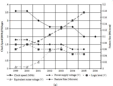
FIG.
4 Developments of integrated circuits and processor families: (a) Moore's
law driving a signal integrity crisis; (b) development of processors and their
power supply requirements; (c) processor speed, power consumption, and equivalent
load impedance.
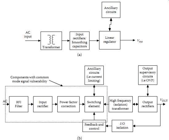
FIG. 5 Comparison of linear power supplies and modern SMPS: (a) simple linear
power supply with an isolation transformer; (b) modern off-the-line switching
power supply and its components vulnerable to common-mode surges.
2.7 Development of DC Power Supplies
During the 1970s and early 1980s, most DC supplies were linear types as depicted in FIG. 5(a). These simple linear power supplies were based on a step-down transformer, which had the advantage of suppressing high-voltage differential- or common-mode transients. Particularly dangerous common-mode transients were easily suppressed by a reasonably well-designed input transformer with galvanic isolation between the windings and with very low interwinding capacitances. If the step-down transformer is designed to have very low interwinding capacitances, the probability of transferring dangerous levels of common-mode transients toward the rectifier stage and the linear regulator chips is pretty low.
FIG. 5(b) depicts the situation of modern SMPS systems designed based on power semiconductors such as BJTs, MOSFETS, or IGBTs where higher VA-rated units carry a power factor correction block as well. In these units essential (regulatory) condition of ground isolation (for minimizing safety issues) is maintained only by the high-frequency switching transformer, which becomes an integral part of the DC-DC converter stage (4). It’s important to note that the input bulk DC rail is created by direct rectification of 230 V/50 Hz or 120 V/60 Hz input source creating an unregulated DC rail of 320 V DC or 165 V DC respectively. Given the complexity of the modern off-the-line SMPS systems, where all circuit blocks from the AC input up to the DC-DC converter stage, there is a disadvantage to having any common-mode signals directly coupled toward the semiconductors. In practice, these systems are much more vulnerable to high-voltage transients, and well-designed surge protection circuits are necessary to protect them.
This is particularly true for the protection of components within the dotted lines of FIG. 5(b).
===
1200 V 900 V 600 V 300 V 400 V Protection level Degradation/ Error or Damage Failure level
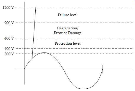
FIG. 6 Transient superimposed on AC-input waveforms with their effects.
===
3 Principles of Surge Protection Techniques
Almost all transients and surges are unpredictable and statistical in nature. It’s not possible to stop them totally, but in planning engineering facilities every effort is made to minimize their effects. However, there is some part of the transients either induced on circuits or directly conducted into the circuits, which can cause disastrous effects on various end user circuits. Protecting a circuit against transients is based on two simple principles: (1) limiting the amplitude of the surge at each component to lower values, and (2) diverting the surge currents through protection-specific components. In practice a designer is expected to protect a system against superimposed surges as shown in FIG. 6. The case is shown for a system where the input supply is 230 V/50 Hz. The voltage spike shown in the figure, which resembles a power surge or a superimposed lightning transient, usually lasts only a few hundred microseconds, compared to the 20 ms-long AC cycle in this case. In the design of the basic power conversion system, the designers disregard the possibility of these superimposed signals and assume that the input utility source is a sinewave as per specifications considered in the project. In general, the possibility of surge damage is related to the height of the spike and the duration of the surge. As indicated in FIG. 6, if the surge peak is between 400 and 600 V, the basic circuit blocks are still considered to be safe. When the spike amplitude is within 600-900 V, degradation of performance or temporary errors could be expected, while values above this can cause permanent faults.
3.1 Practical Devices Used in Surge Protection Circuits
In developing surge protection circuits, based on the simple concepts discussed above the designer has to look after two important aspects, namely: (1) surge arrestor stages inserted should not alter the normal operation of the power conversion circuit; (2) components used for surge absorption, diversion, or attenuation should withstand the surges safely. Reliability of the surge protection system is another important concern, since in practical circumstances if a very high level surge enters the system, it might kill the surge arrestor itself.
In designing practical surge arrestor circuits, nonlinear devices such as metal oxide varistors (MOVs), and semiconductor devices such as thyristors or avalanche-type zeners are combined with inductors and capacitors. Gas discharge tubes (GDTs) are also used in some systems.
3.1.1 Gas Discharge Tubes
Gas discharge tubes (GDTs, or simply gas tubes) are devices that employ an internal inert gas that ionizes and conducts during a transient event. Because the internal gas requires time to ionize, gas tubes can take several microseconds to turn on or "fire." In fact, the reaction time and firing voltage are dependent on the rising slope of the transient front. A circuit protected by a gas tube arrestor will typically see overshoot voltages ranging from a few hundred volts to several thousand volts. These devices are available for protection of AC line input as well as signal and communication circuits.
3.1.2 Metal Oxide Varistors
Metal oxide varistors (MOVs) are devices composed of ceramic-like material usually formed into a disk shape. They are typically constructed from zinc oxide plus a suitable additive. Each inter-granular boundary displays a rectifying action and presents a specific voltage barrier. When these conduct, they form a low ohmic path to absorb surge energy (5). A varistor's voltage-current behavior is defined by the relationship:
I = KVα
…where K and α are device constants. K is dependent on the device geometry, and α defines the degree of nonlinearity in the resistance characteristic and can be controlled by selection of materials and the manufacturing process. High α implies a better clamp, and zinc-oxide technology comes with α values in the range of 15-30. High transient energy absorbent capability is achieved by increasing the size of the disc. Typical sizes range from 3 to 20 mm in diameter. MOVs turn on in a few nanoseconds and have high clamping voltages, ranging from approximately 30 V to 1.5 kV. FIG. 7 compares the behavior of an MOV with an ideal clamping device and with a solid-state device like a transient voltage suppressor (TVS) zener diode. For more implementation details on MOVs, ( 6, 7) are suggested. For basic theory of operation of ZnO varistors, (22, 23) are suggested.
Subjecting an MOV to continuous abnormal voltage conditions rather than short-duration transients may cause the MOV to go into thermal runaway, resulting in overheating, smoke, and even potential fire. To prevent this condition, many modern MOVs include an internal thermal fuse or a thermal cutoff device. Some even extend this capability with an internal indicator that provides a logic output if the device's thermal protection is engaged (12). An overview comparison of thermally protected MOVs (TPMOVs) with traditional MOVs is provided in (13). These TPMOVs are useful in occasions where continuous AC line overvoltages could occur.
===
Current _rough the Device (I) Clamping voltage; Working voltage; Voltage Across the Device (V) Protection region Clamping voltage Working voltage Current _rough the Device (I) Voltage Across the Device (V) Protection region Clamping voltage (Zener voltage) Working voltage Current _rough the Device (I) Voltage Across the Device (V) Protection region (c)
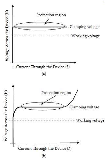
FIG. 7 Comparison of transient protection devices: (a) ideal case; (b) zinc-oxide
varistor; (c) TVS zener diode.
===
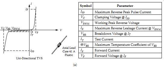
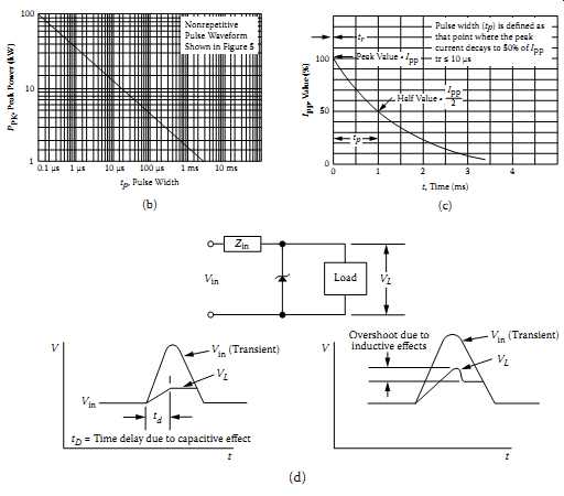
FIG.
8 An example of a TVS diode: (a) device behavior and data sheet parameters;
(b) pulse power absorption capability versus pulse width; (c) test pulse used;
(d) typical application circuit and voltage at protected load due to device
capacitance and lead inductance.
===
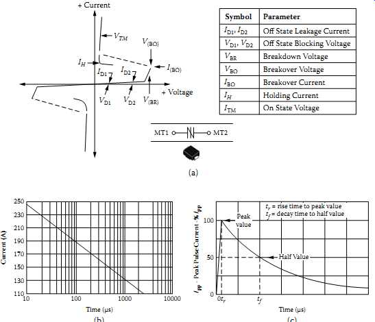
FIG. 9 An example of a thyristor breakover device: (a) device behavior and
data sheet parameters; (b) pulse power absorption capability versus pulse
width; (c) test pulse used; (d) typical application circuit in telecommunication
plant with series current-limiting device.
===
TBL. 1 Comparison of TVS Devices
Suppression Element Advantages Disadvantages Expected Life Gas tube Very high current-handling capability Low capacitance High insulation resistance Very high firing voltage Finite life cycle Slow response times Non-restoring under DC Limited MOV High current-handling capability Broad current spectrum Broad voltage spectrum Gradual degradation High clamping voltage High capacitance Degrades TVS diodes Low clamping voltage Does not degrade Broad voltage spectrum Extremely fast response time Limited surge current rating High capacitance for low-voltage types Long limited TVS thyristors Does not degrade Fast response time High current-handling capability Non-restoring under DC Narrow voltage range Turn-off delay time Long
===
3.1.3 Solid-State Devices
Two basic types of solid-state devices for surge absorption are available. TVS diodes are solid-state p-n junction devices. Both these types are available as back-to-back devices (bidirectional devices) suitable for protection against positive or negative surges appearing at power or signal entry inputs.
Compared to a zener, which is designed to regulate a steady-state voltage, the TVS diode is designed to clamp a transient surge voltage. A large cross-sectional area is employed for a TVS diode junction, allowing it to conduct high-transient currents. These diodes respond almost instantaneously to transient events. Their clamping voltage (which is the voltage measured across the device terminals when the device is fired, and a peak pulse current is flowing through the device) ranges from a few volts to a few hundred volts, depending on the breakdown voltage of the device. The fast response time of the TVS diodes means that any voltage overshoot is primarily due to lead inductance. FIG. 8 provides an example of a commercial device from ON Semiconductor (8). Data sheet terminology for silicon TVS devices, and design calculations are discussed.
TVS thyristors are solid-state devices constructed with four alternating layers of p-type and n-type material. The resulting device is capable of handling very high pulse currents. These devices respond in nanoseconds and have operating voltages that start at about 28 V and go up. FIG. 9 provides an example of a commercial device from ON Semiconductor, with a typical telecommunication outside plant protection circuit (9).
The ability of TVS diodes to dissipate surge voltages that contribute to the early failure of semiconductors can be evaluated using SPICE macromodels (10).
TBL. 1 compares the characteristics of the most widely used TVS devices.
3.2 Levels of Surge Protection
TVS device protection levels may be divided into three categories: (a) primary protection, (b) secondary protection, and (c) board-level protection.
3.2.1 Primary Protection
Primary protection applies to power lines and data lines exposed to an outdoor environment, service entry, and AC distribution panels. Transient currents can range from tens to hundreds of kiloamps at these sources.
3.2.2 Secondary Protection
Secondary protection is for equipment inputs, including power from long-branch circuits, internal data lines, PBX, wall sockets, and lines that have primary protection at a significant distance from the equipment. Transient voltages can exceed several kilovolts with transient currents ranging from several hundred to several thousand amps.
3.2.3 Board-Level Protection
Board-level protection is usually internal to the equipment; it’s for protection against residual transient from earlier stages of protection, system-generated transients, and electrostatic discharge (ESD). Transients at this level range from tens of volts to several thousand volts with currents usually in the tens of amps.
3.3 Circuit Concepts Used for Surge Protection
In general practical circuits developed for surge protection are based on few simple concepts:
(1) design the protection circuit separately as an add-on block to the base circuit;
(2) attenuate the incoming transient using passive series impedances, or bypass the surge currents via passive low-impedance circuits (they act as filters for high-frequency components of the surge); (3) use nonlinear devices such as GDTs, MOVs, or TVS to divert the surge currents and absorb the transient energy. FIG. 10 depicts four different kinds of TVSS circuits.
In FIG. 10(a), which is designed to protect against both common and differential mode transients, M1 to M3 are MOVs that will enter their firing or conduction mode when the transient exceeds the threshold voltage limit. Inductors L1 and L2 act as high impedances for the transient signal, since its spectrum contains many higher-frequency components, compared to the impedance of the inductors at the line frequency. Similarly, the capacitors indicated as Cnx and Cny act as low-impedance paths to the transient signal, which helps divert the transient energy from reaching the critical load end. The overall effect of these circuitry is to minimize the transfer of the transient voltage toward the critical load side. However, due to clamping voltages of the MOVs, some share of the transient energy reaches the load side. The TVS diodes (or thyristors) are used to absorb the remaining transient energy to minimize the possible damage. FIG. 10(b) indicates a communication line protection scheme, and FIG. 10(c) is an example of line driver/receiver protection. FIG. 10(d) is an example of generic IC protection.
FIG. 11(a) indicates the typical V-I characteristics of an MOV. At low currents the V-I curve approaches a linear ohmic relationship and shows a significant temperature dependence (11). Under this condition the MOV is in a very high resistance mode, approaching about 1 GΩ or higher. Under this near-open-circuit condition, the nonlinear resistance RX in FIG. 11(b) can be ignored, as ROFF value in parallel will dominate.
FIG. 11(c) indicates equivalent circuits under off and conduction states, as applicable in a design calculation. ROFF value is dependent on the temperature, but remains in the range of 10-1000 MΩ. It also depends on the frequency in an inversely proportional manner. Under conduction mode the value of RX in FIG. 11(c) becomes many orders of magnitude less than the ROFF value. The effect of this MOV set in FIG. 10(a) is to absorb much of the transient energy into the MOVs if a common- or differential-mode transient occurs.
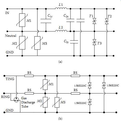
FIG. 10 Different types of surge protection circuits: (a) multistage surge
suppressor (SS) using a combination of devices; (b) communication or signal
line protection using multistage SS devices including a GDT; (c) line driver-receiver
protection using back-to-back thyristor elements. (d) generic IC protection.
4 Surge Protection Standards and Practices
Transients that could induce on the equipment inputs could be due to several different categories such as (a) inductive switching, (b) lightning, (c) electrostatic discharge, and (d) electromagnetic pulses (EMPs). All these are very unpredictable random occurrences.
Electrostatic discharge may occur due to buildup of static charge on human body up to voltages as high as 20,000 V. These can generate transients with rise times as high as 2 kV/ns. Electromagnetic pulses due to nuclear activities where gamma rays can be released could cause transients with rise times with 5 kV/ns, while lightning activity related transients can generate signals with rise times around 600 V/ns (17). Due to the statistical nature of the transient voltages superimposed, many useful guidelines are provided by the standards and practices available for the designers. Transient activity can be divided into external sources and internal sources.
4.1 External Sources of Transient Activity
Power companies have no control over transients induced by lightning or high-power switching at substation levels. FIG. 12 illustrates the enormous energy content of a typical lightning waveform. Currents from a direct or indirect strike may enter conductors of a suspended cable or enter a buried cable by ground currents. Either way, the surge will propagate in the form of a traveling wave bi-directionally on the cable from the point of origin. Severity of impact to the end user is directly proportional to the proximity of the lightning strike. If the facility is at a 10-20 pole distance from the strike, little harm will occur, since the surge current will have been dissipated by the utility ground system. Such is not the case where the strike is much closer. In this case, the residual current can migrate through the facility's service equipment and cause severe damage.
Other externally generated transients result from switching in nearby industrial complexes, which can send transients back into the power line, causing damage to equipment.
EMPs are another rare case of external transient activity.
4.2 Internal Sources of Transient Activity
Internally generated transients result from switching within the facility. Any time the flow of inductive currents is altered, such as in the simple act of turning a motor or when a fluorescent light with a magnetic choke is on and off, transient activity can result in an "inductive kick." An excellent example of this phenomenon in day-to-day life is the transients generated by turning off a fluorescent light with a magnetic ballast.
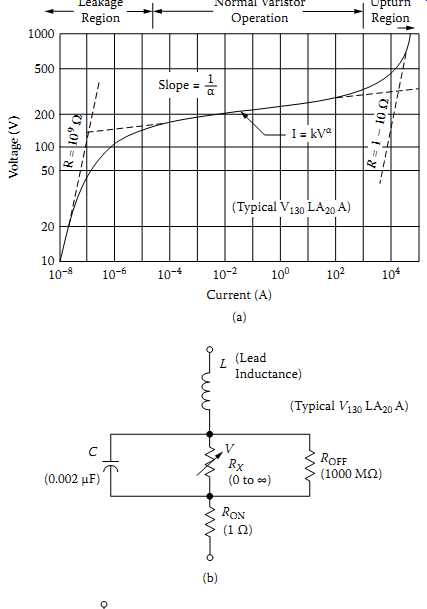
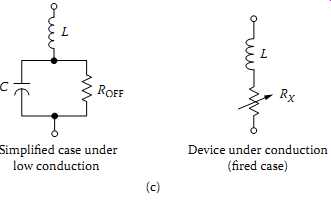
FIG. 11 Metal oxide varistor characteristics and equivalent circuits: (a)
V-I characteristics; (b) generalized equivalent circuit; (c) simplified cases
under low conduction and fired cases.
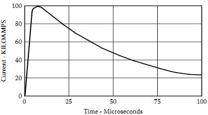
FIG. 12 A typical lightning current waveform.
4.3 Transient Energy
The energy of a transient waveform may be readily calculated for transients that are internal to the circuit, such as those caused by inductive switching. Transients external to the circuit are more difficult to quantify. The energy absorbed by the suppression element may be approximated by:
…where, E = energy in joules; Vc = clamping voltage in volts; Ip = peak pulse current in amperes; and τ = impulse duration.
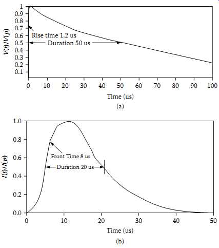
FIG. 13 Surge waveforms: (a) open-circuit voltage waveform; (b) discharge
current waveform; (c) ring waveform for testing long branch circuits.
4.4 Transient Protection Standards
Committees such as ANSI, IEEE, and IEC have defined standards for transient wave shapes based on the threat environment. European or IEC transient standards include:
• IEC 61340-3-1 Electrostatics: Methods for simulation of electrostatic effects- human body model (HBM) electrostatic discharge test waveforms
• IEC 61340-3-2 Electrostatics: Methods for simulation of electrostatic effects - Machine model (MM) electrostatic discharge test waveforms
• IEC 61000-4-4 Electromagnetic compatibility (EMC): Testing and measurement techniques - Electrical fast transient/burst immunity test
• IEC 61643 series - For low voltage surge protection U.S. transient standards include:
• ANSI/IEEE C62.4x series for power line transients
• FCC Part 68 for telecommunication lines
• UL 1449 and various military standards
In all these standards, the transient wave shape is usually defined as an exponentially decaying pulse or a ring wave (damped sinusoidal) for electrical surges. The exponentially decaying open-circuit voltage and short-circuit current waveforms are shown in Figures 13(a) and 13(b), respectively. These impulse waveforms are defined by their rise times and half-amplitude duration. For example, an 8 × 20 μsec impulse current would have an 8 μsec rise time from 10% of the peak current to 90% of the peak current. A 20 μsec time is measured between half-amplitude points. The ring wave results from the effect of a fast rise time transient encountering the impedance of a wiring system.
The waveform shown in FIG. 13(c) is a 100 kHz ring wave with an initial rise time of 0.5 μsec. The wave shape is defined as rising from 10% to 90% of its peak amplitude in 0.5 μsec and decaying while oscillating at 100 kHz. Each peak is 60% of the amplitude of the preceding one. Most surge protection component data sheets define the surge capability of a suppression device using an 8 × 20 μsec or 10 × 1000 μsec current waveform.
===
TBL. 2 C62.41 Location Categories, Frequency of Occurrences, and Surge Waveforms
IEEE LOCATION CATEGORY IEEE EXPOSURE 2000 Volt, 70 Ampere Ringwave Surges (0.63 Joules) 4000 Volt, 130 Ampere Ringwave Surges (2.34 Joules) 6000 Volt, 200 Ampere Ringwave Surges (5.4 Joules) A1 Low 0 0 0 A2 Medium 50 5 1 A3 High 1000 300 90 2000 Volt, 1000 Ampere Combination Wave Surges (9 Joules) 4000 Volt, 2000 Ampere Combination Wave Surges (36 Joules) 6000 Volt, 3000 Ampere Combination Wave Surges (81 Joules) B1 Low 0 0 0 B2 Medium 50 5 1 B3 High 1000 300 90
===
4.5 IEEE C62.41 : "IEEE Recommended Practice on Characterization Surge in Low-Voltage (1000 V) and less AC Power Circuits"
IEEE C62.41 identifies location categories within a building, described such as A1, A2, A3, B1, B2, and B3 for surge locations. The "A" and "B" location prefixes represent wiring run distances within a building; the "1," "2," and "3" suffixes represent surge severity. "A" category locations receive their power after more than 60 ft. of wiring run from the main power service entrance, with frequent exposure to comparatively low-energy surges.
External surges will be of a lesser threat in "A" locations than "B" locations due to the impedance protection provided by the inductance of the building wiring in "A" locations.
IEEE specifies a low-energy "ringwave" surge waveform for the "A" locations.
"B" category locations are within a building, close to the power service entrance, with greater exposure to infrequent, high-energy surges originating outside the building. The
"B" location category surges can be caused by lightning, power outages due to storms, and normal utility switching functions. A "combination wave" with high surge energy is specified by IEEE for these "B" locations.
"1," "2," and "3" denote low, medium, and high exposures respectively, in terms of the number and severity of surges, with "1" being the least severe and "3" being the most severe. A "B3" location, therefore, would have the highest exposure to surge energy, while an "A1" location would have the lowest incidence of surge energy.
TBL. 2 shows possible annual surge magnitudes, frequency of occurrences, and surge waveform as extracted from the IEEE C62.41 Standard. FIG. 14 depicts the building locations, the probabilistic nature of surge severity, and the possibility of upset or damage to systems due to surge. The reader is expected to refer to the set of C62.XX series standards such as C62.41.2 for details.
====
Increasing surge severity; level; Probability of upset or damage due to surge (Manufacturer specified); Relative frequency of occurrence of surges; Upset; Damage
UL1449-Type 1 UL 1449-Type 2 UL 1449-Type 3 Category C - Secondary side of the service transformer drop to the line side of the main overcurrent protection device. .is a critical location to apply surge protection in order to stop external surges before they get in.
Category B - Load side of the main overcurrent protection device to distribution panels Category A - Branch and receptacle locations; IEEE C62 Categories
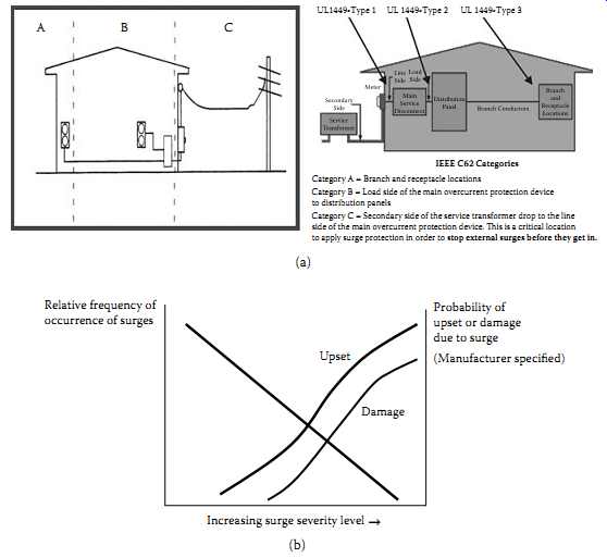
FIG. 14 Building locations and severity of surge: (a) categories A to C;
(b) severity of surge and upset or damage probability.
====
4.6 Underwriters Laboratories UL 1449
About two decades ago, Underwriters Laboratories (UL) established a uniform TVSS rating system by creating UL Standard 1449-1987. Although somewhat limited, it was the first step toward establishing benchmarks by which to compare TVSS products. UL established specific test criteria to determine the ability of a TVSS product to stop the travel of a transient voltage surge into protected equipment. TVSS devices were divided into two categories: plug-in or cord-connected devices, and hardwired or direct-connected devices. The plug-in and cord-connected category is subjected to a maximum transient surge impulse of 6000 V with a short-circuit current of 500A available. The voltage available is in a 1.2 × 50 μs waveform, and the current is available in an 8 × 20 μs waveform.
Devices included in the hardwired category are subjected to an impulse of 6000 V with 3000 A available in the same type of waveform (19). In the latest revision of the standard, published in September 2006, the title is changed to "UL Standard for Safety for Surge Protective Devices, UL 1449." This third edition has become a standard by ANSI. In this new edition, the commonly used term TVSS is replaced by surge protective devices (SPDs), and the new test and currents are revised upwards by a factor of six, bringing the test conditions in the let-through voltage tests to 3 kA from 0.5 kA with the same open-circuit voltage of 6 kV. Also, it assigns Type 1 to Type 3 related to C62.41 categories, corresponding to category C to category A. The right-hand side of FIG. 14(a) indicates this relationship in a practical situation. Type 4 applies to individual components used in all location categories. More details can be found in (20, 21).
4.7 Electrostatic Discharge and Circuit Protection
Electrostatic discharge (ESD) is a serious issue in the assembly and testing of systems containing semiconductor devices. There are various standards developed for testing the ESD capability of semiconductor products. These standards have been generated with regard to a specific need related to the electromagnetic compatibility of the system environment. They include the human body model (HBM), machine model (MM), and charged device model (CDM). Each such standard relates to the nature of electrostatic discharge generated within a system application and the potential for damage to the IC.
Among the better known standards are:
• Human body model using the MIL-STD-883, Method 3015.7
• Machine model using EIAJIC121
• Human body model using the IEC 1000-4-2 standard Testing for ESD immunity is more broadly defined to include a device, equipment, or system. Both direct-contact and air discharge methods of testing are used with four discrete steps in the severity level ranging up to 8 KV and 15 kV, respectively. In its simplest form, the FIG. 15(a) test circuit provides a means of charging the 150 pF capacitor, RC, through the charge switch and discharging ESD pulses through the 330
Ω resistor, RD, and discharge switch to the equipment or device under test. The test equipment for the IEC 1000-4-2 standard is constructed to provide the equivalent of an actual human body ESD discharge and has the waveform shown in FIG. 15(b).
4.8 Protection of Printed Circuit Board Components
As we discussed earlier, any remaining components of a transient or an ESD can ultimately end up on a PCB, physically destroying its components or temporarily corrupting any stored data. In order to safeguard physical components in PCBs, semiconductor manufacturers such as Littelfuse and ON Semiconductor have introduced components suitable for board-level protection. Two basic component solutions exist. They are TVS diode arrays and SCR-diode arrays, which come in common IC packages. These devices cater to ESD protection requirements in general.
The SP720, SP721, and SP723 are protection ICs from Littelfuse with an array of SCRdiode bipolar structures for ESD and overvoltage protection of sensitive input circuits.
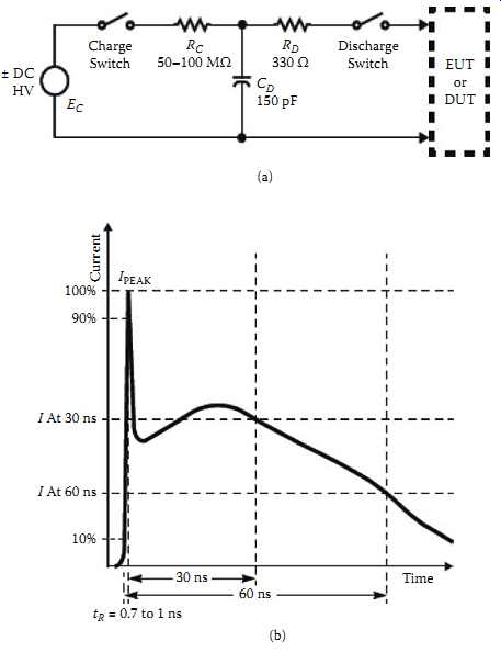
FIG. 15 ESD test energy source and output current of an ESD generator. (a)
test system (b) waveform
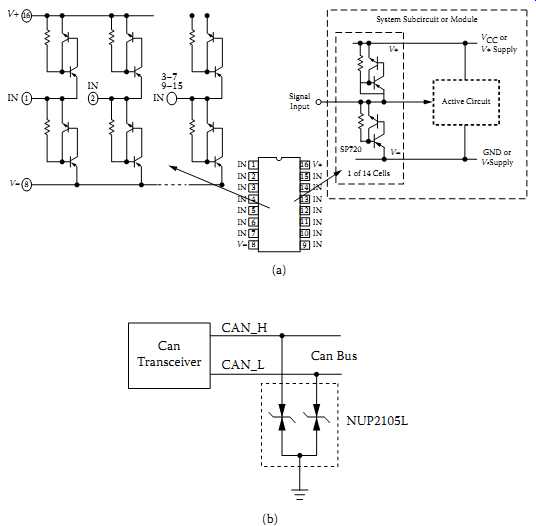
FIG. 16 ESD protection and techniques: (a) use of SCR-type device arrays;
(b) use of TVS diodes.
They have two protection SCR-diode device structures per input. See FIG. 16(a). The SCR structures are designed for fast triggering at a threshold of one +VBE diode threshold above +V (positive supply terminal) or a -VBE diode threshold below V- (negative or ground). A clamp to V+ is activated at each protection input if a transient pulse causes the input to be increased to a voltage level greater than one VBE above V+. A similar clamp to V- is activated if a negative pulse, one VBE less than V-, is applied to an input.
Similar to the case of SCR-type devices, the TVS diode is also an effective low-cost option to protect sensitive devices from ESD and EMI. In these cases the devices are connected between signal lines and a ground connection or a ground plane on a PCB.
Typical examples are the NUP 2105 from ON Semiconductor (26), which is typically used in automotive CAN bus environments and the like. Usually the device connection is as shown on FIG. 16(b), where the diodes provide common-mode paths between the signal lines and the ground.
5 Practical Design Considerations
Having discussed a background on surge protection devices and practices, it’s also important to discuss the PCB layout and assembly issues, since these could enhance or degrade the level of protection provided by the devices, particularly in the case of board-level protection. In developing board-level protection stages, we have to keep in mind that capacitive and inductive parasitic elements in a PCB can compromise the level of protection offered by the device such as a TVS diodes, or a TVS thyristor structure, which comes in compact IC packages or as individual elements.
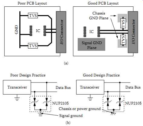
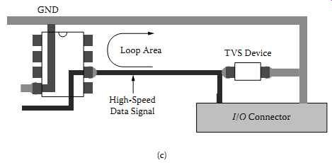
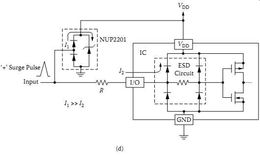
FIG. 17 PCB Layout issues: (a) good and bad practices in placing the TVS
device closer to I/O connector with minimum inductive traces; (b) good and
bad practices in using the correct ground return, when separate signal and
chassis grounds exist; (c) data and ground traces forming a loop, which could
act as an antenna with increased RF susceptibility; (d) use of resistor to
absorb the majority of surge energy by the external diodes.
In general TVS devices should be used on all data and power lines that enter or exit a PCB at the I/O connector. Locating the TVS devices as close as possible to the noise source ensures that a surge voltage will be clamped before the pulse can be coupled into any adjacent PCB traces. FIG. 17(a) depicts this scenario, indicating the good and bad practices. In general the TVS device should be very close to the I/O connector and minimizing the length of the TVS traces. In the figure on the left-hand side, due to inductances of the traces part of the energy in the surge pulse can be entering the IC.
Unless this component can be absorbed by the ESD protection stages inside the IC, it can have disastrous consequences. The figure on the right-hand side indicates a multilayer PCB, where a separate GND plane is used where return end of the TVS diode is connected, to minimize any inductive impedance. It’s simply important to remember that a short trace length equates to a low impedance, which ensures that the surge energy will be dissipated by the TVS device instead of the IC's internal ESD protection stage.
Locating sensitive traces in the center rather than near the edge of the PCB is a simple method to protect against any ESD issues during handling.
It’s important to consider that when a transient is diverted by a TVS device, it can cause a significant current to flow through the device into ground connection or the ground plane. This high current can cause a momentary voltage spike on the ground paths, which can have complex connections within the PCB. In cases where the signal and chassis grounds are separately laid out, if the surge transient-related currents are returned to chassis ground, it may not create a significant transient voltage rise on the signal path ground. FIG. 17(b) depicts the good and bad practices, noting the two independent GND connections in the right-hand figure. In the left-hand figure, shunting the surge voltage directly to the IC's signal ground can cause ground bounce.
As shown in FIG. 17(c), another possible issue is the radio frequency susceptibility issue due to loop area formed by high-speed signal lines and the ground return paths. One effective method to minimize this loop problem is to incorporate a separate ground plane.
In FIG. 17(c), we can see that the maximizing the separation distance from the TVS device in IC provides isolation, however, at the expense of forming a larger loop area.
FIG. 17(d) indicates a case of a diode set such as NUP 2201 from ON Semiconductor used with a semiconductor chip where ESD protection is built in. In such cases, placing a series resistor, such as R in FIG. 17(d), ensures that the majority of surge energy is absorbed by the external TVS diode. More details on device selection guidelines and placement options are discussed. ESD failure modes and mechanisms are discussed.